
SiC JBS cellular structure and preparation method thereof

A cell and graphic technology, applied in the field of SiCJBS cell structure and preparation, can solve the problem of unbalanced leakage current and anti-surge current ability, achieve improved anti-surge current ability, wide application range, and increase inrush current Effect

Active Publication Date: 2022-01-28
XIAN MICROELECTRONICS TECH INST
View PDF16 Cites 0 Cited by
  • Summary
  • Abstract
  • Description
  • Claims
  • Application Information

AI Technical Summary

Problems solved by technology

[0005] Aiming at the problems existing in the prior art, the present invention provides a SiC JBS cell structure and preparation method, which effectively solves the problem of insufficient leakage current and anti-surge current capability when the cells of the JBS structure and the Schottky region are alternately arranged. balance problem

Method used


Image

  • SiC JBS cellular structure and preparation method thereof
  • SiC JBS cellular structure and preparation method thereof

Examples


Embodiment 1

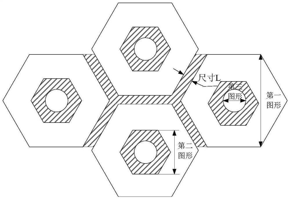
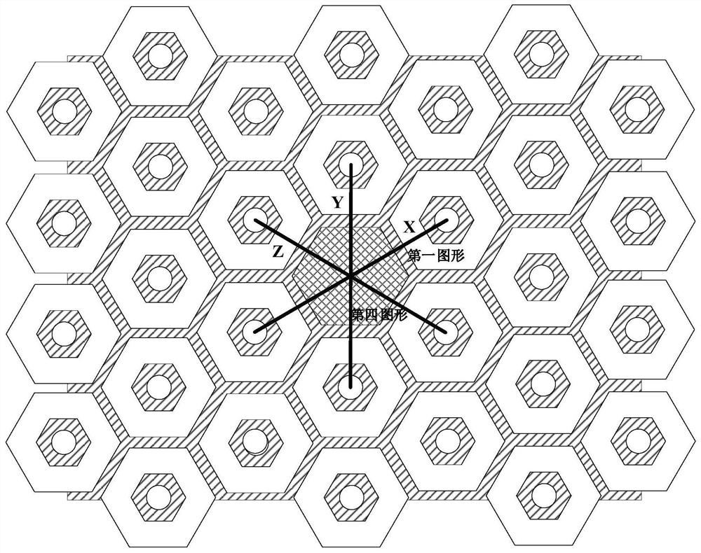
[0058] A SiC JBS cell structure of the present invention includes the following steps: first, deposit an oxide layer on the SiC epitaxial layer to form an implanted masking region; then, carry out photolithography of cell patterns on the oxide layer, such as figure 1 As shown, the first cell and the second cell; the periphery of the second cell is arranged with several first cells; the cross section of the filling area of ​​the first cell is the third figure from the inside to the outside, the first The second figure, the first figure; the area type corresponds to SBD area, P+ area, SBD area or P+ area, SBD area, P+ area in turn; the cross section of the filled area of ​​the second cell is the fourth figure, and the area type is P-type doped region; the first figure is a regular hexagon, the second figure is a regular hexagon, the third figure is a circle or a regular hexagon, and the fourth figure is a regular hexagon. The geometric size of the first figure in the cell is 25u...

Embodiment 2

[0062] A SiC JBS cell structure of the present invention includes the following steps: first, deposit an oxide layer on the SiC epitaxial layer to form an implanted masking region; then, carry out photolithography of cell patterns on the oxide layer, such as figure 1 As shown, the first cell and the second cell; the periphery of the second cell is arranged with several first cells; the cross section of the filling area of ​​the first cell is the third figure from the inside to the outside, the first The second figure, the first figure; the area type corresponds to SBD area, P+ area, SBD area or P+ area, SBD area, P+ area in turn, the cross section of the filled area of ​​the second cell is the fourth figure, and the area type is P-type doped region; the first figure is a regular hexagon, the second figure is a regular hexagon, the third figure is a circle or a regular hexagon, and the fourth figure is a regular hexagon. The geometric size of the first figure in the cell is 100...

Embodiment 3

[0064] A SiC JBS cell structure of the present invention includes the following steps: first, deposit an oxide layer on the SiC epitaxial layer to form an implanted masking region; then, carry out photolithography of cell patterns on the oxide layer, such as figure 1 As shown, the first cell and the second cell; the periphery of the second cell is arranged with several first cells; the cross section of the filling area of ​​the first cell is the third figure from the inside to the outside, the first The second figure, the first figure; the area type corresponds to SBD area, P+ area, SBD area or P+ area, SBD area, P+ area in turn, the cross section of the filled area of ​​the second cell is the fourth figure, and the area type is P-type doped region; the first figure is a regular hexagon, the second figure is a regular hexagon, the third figure is a circle or a regular hexagon, and the fourth figure is a regular hexagon. The geometric dimension L of the first figure in the cell...


PUM


Abstract

A SiC JBS cellular structure comprises first cells and a second cell; a plurality of first cells are arranged on the periphery of the second cells; the cross sections of the filling area of the first cells are sequentially provided with a third pattern, a second pattern and a first pattern from inside to outside; the area types sequentially correspond to an SBD area, a P + area and an SBD area or sequentially correspond to the P + area, the SBD area and the P + area; the cross section of the filling area of the second cell is a fourth pattern, and the region type is a P-type doped area; and the first graph is a regular hexagon, the second graph is a regular hexagon, the third graph is a circle or a regular hexagon, and the fourth graph is a regular hexagon. According to the invention, the size of SiC-JBS pain current is controlled by controlling the geometric dimension of the pattern of the cellular structure and the relative distance between the cells, and the purpose of increasing surge current is achieved by reasonably distributing the P + region.

Description

technical field [0001] The invention belongs to the technical field of power device design, and relates to a SiC JBS cell structure and a preparation method. Background technique [0002] Silicon carbide (SiC) is a binary semiconductor compound. It is the only solid compound among the elements of the IV main group of the periodic table and the only stable compound of Si and C. Its physical and chemical properties have many unique features. When the SiC material is crystallized, each carbon atom is closely surrounded by 4 silicon atoms according to the regular tetrahedral structure, and each silicon atom is also closely surrounded by 4 carbon atoms in the same way, nesting each other to form a complete crystal . The nearest neighbor atomic distance is 0.189nm, so the roughness at the SiC atomic level is about 0.2nm. Silicon carbide crystals conform to the principle of close packing in the process of crystallization and structure, and the hardness of SiC material is high, se...

Claims


Application Information

Patent Timeline
Patent Type & Authority Applications(China)
IPC IPC(8): H01L29/06H01L29/872H01L21/04
CPCH01L29/0692H01L29/0607H01L29/872H01L21/0445H01L29/6606Y02P70/50
Inventor 侯斌杨晓文杨鹏翮鲁红玲李照黄山圃胡长青
Owner XIAN MICROELECTRONICS TECH INST
Learn More