A detection method for pcb board soldering defects based on depth information
A PCB board and soldering defect technology, applied in the field of electronic component detection, can solve the problems of slow processing speed, excessive data volume, high false detection rate, etc., to reduce false detection rate, reduce data volume, and lower lighting conditions Effect
- Summary
- Abstract
- Description
- Claims
- Application Information
AI Technical Summary
Problems solved by technology
Method used
Image
Examples
Embodiment Construction
[0020] In order to make the technical means, creative features, goals and effects achieved by the present invention easy to understand, the present invention will be further described below in conjunction with specific embodiments.
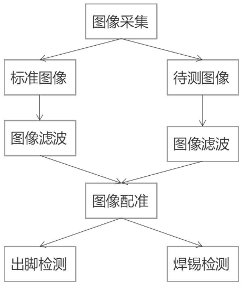
[0021] Such as figure 1 Shown, a kind of PCB board welding defect detection method based on depth information, described method comprises the following steps:
[0022] Collect the depth data of the welding area of the PCB board to be tested and the welding area of the standard PCB board respectively, use the line laser to scan the front and back of the standard PCB board, and collect the depth data of the front and back sides of the board;
[0023] According to the depth data of the welding area of the two PCB boards, corresponding depth images are generated respectively;
[0024] Obtain the standard welding image according to the depth image of the standard PCB board, obtain the welding image to be tested according to the depth image of th...
PUM
 Abstract
Description
Claims
Application Information
