Supercharge Your Innovation With Domain-Expert AI Agents!

Three-dimensional semiconductor device including vertical structures

A vertical structure and semiconductor technology, applied in the direction of semiconductor devices, transistors, electric solid-state devices, etc., can solve the problem of increased difficulty in gate formation process

Pending Publication Date: 2019-05-28
SAMSUNG ELECTRONICS CO LTD
View PDF0 Cites 1 Cited by
  • Summary
  • Abstract
  • Description
  • Claims
  • Application Information

AI Technical Summary

Problems solved by technology

As described above, as the number of gate electrodes stacked in the direction perpendicular to the surface of the semiconductor substrate increases, the degree of difficulty of the gate formation process gradually increases, and unexpected defects occur

Method used


Image

  • Three-dimensional semiconductor device including vertical structures
  • Three-dimensional semiconductor device including vertical structures
  • Three-dimensional semiconductor device including vertical structures

Examples


Embodiment Construction

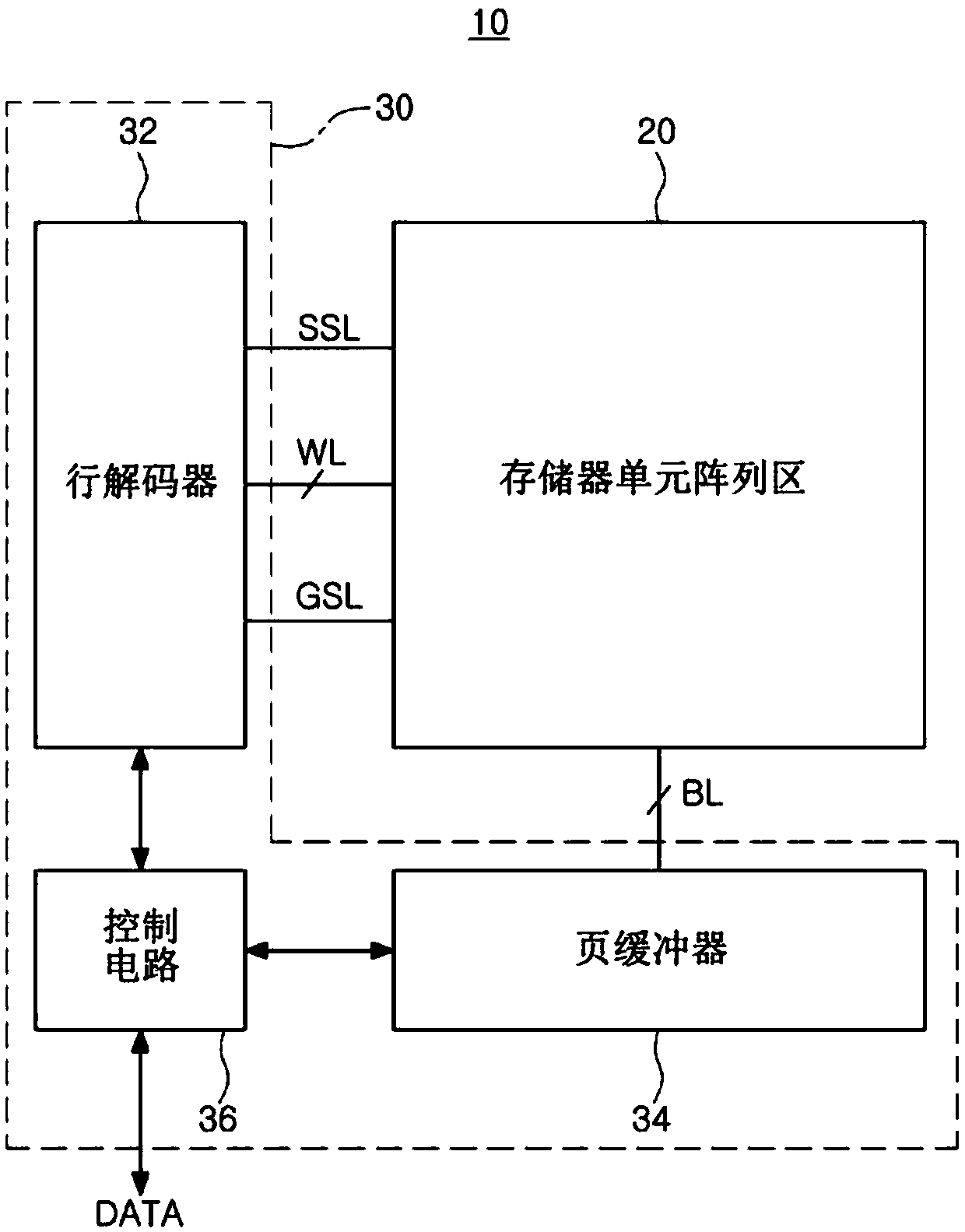
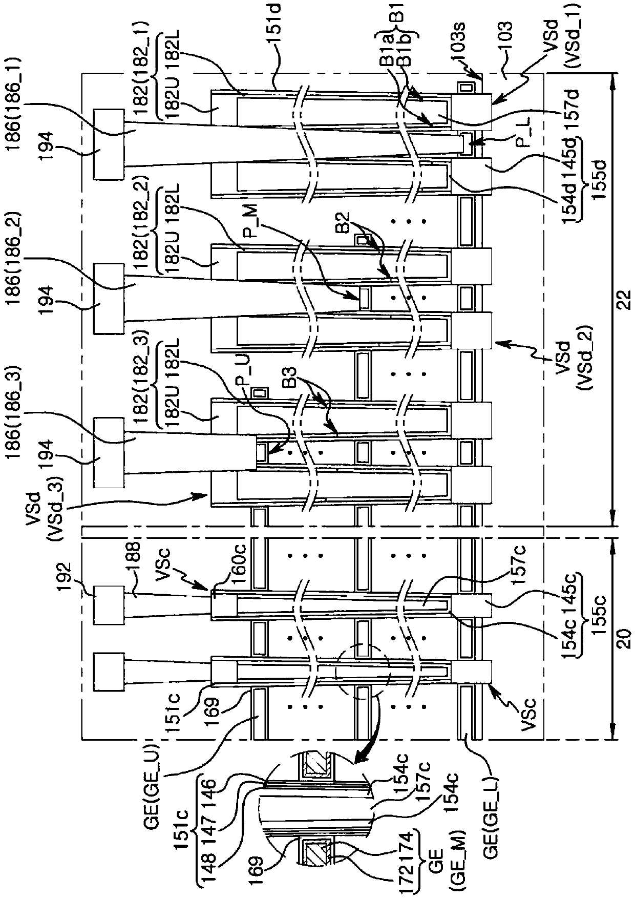
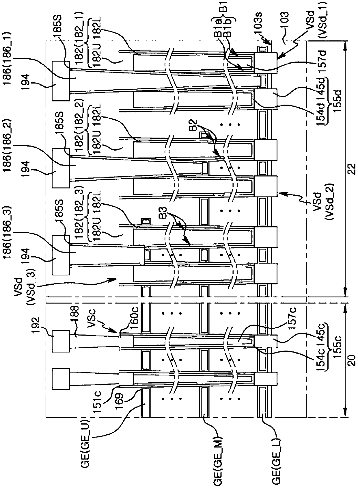
[0024] Various example embodiments will be described more fully hereinafter with reference to the accompanying drawings, in which some example embodiments are shown. Inventive concepts may, however, be embodied in many different forms and should not be construed as limited to the example embodiments set forth herein. Rather, these example embodiments are provided so that this description will be thorough and complete, and will fully convey the scope of the inventive concept to those skilled in the art. In the drawings, the size and relative sizes of layers and regions may be exaggerated for clarity.

[0025] It will be understood that when an element or layer is referred to as being "on," "connected to," or "coupled to" another element or layer, it can be directly on the other element or layer. An element or layer may be on, connected to, or bonded directly to another element or layer, or intervening elements or layers may be present. In contrast, when an element or layer is...


PUM


Abstract

A three-dimensional semiconductor device is provided including a gate electrode disposed on a substrate and having a pad region; a cell vertical structure passing through the gate electrode; a dummy vertical structure passing through the pad region; and a gate contact plug disposed on the pad region. The cell vertical structure includes a cell pad layer disposed on a level higher than that of thegate electrode and a cell channel layer opposing the gate electrode, the dummy vertical structure includes a buffer region formed of a material different from that of the cell pad layer and a dummy channel layer formed of a material the same as that of the cell channel layer, and at least a portion of the buffer region is located on the same plane as at least a portion of the cell pad layer.

Description

[0001] This application claims the benefit of priority from Korean Patent Application No. 10-2017-0154892 filed in the Korean Intellectual Property Office on November 20, 2017, the disclosure of which is hereby incorporated by reference in its entirety. technical field [0002] The inventive concept relates to a semiconductor device, and more particularly, to a three-dimensional semiconductor device including a vertical structure passing through a gate electrode. Background technique [0003] Semiconductor devices including gate electrodes stacked in a direction perpendicular to the surface of a semiconductor substrate have been developed. For high integration of semiconductor devices, the number of stacked gate electrodes has increased. As described above, as the number of gate electrodes stacked in the direction perpendicular to the surface of the semiconductor substrate increases, the degree of difficulty of the gate formation process gradually increases, and unexpected d...

Claims


Application Information

Patent Timeline
IPC IPC(8): H01L27/11582H01L27/11573
CPCG11C7/18H10B43/35H10B43/10H10B43/40H10B43/27H01L29/788H10B41/40H10B41/20H10B41/30H01L29/42328G11C16/08G11C8/10H10B41/27H10B41/35
Inventor 郑煐陈
Owner SAMSUNG ELECTRONICS CO LTD
Features
  • R&D
  • Intellectual Property
  • Life Sciences
  • Materials
  • Tech Scout
  • Unparalleled Data Quality
  • Higher Quality Content
  • 60% Fewer Hallucinations
Learn More