Forming method of three-dimensional memory device, and three-dimensional memory device

A three-dimensional storage and device technology, applied in semiconductor devices, electrical solid devices, electrical components, etc., can solve problems such as device defects

Active Publication Date: 2019-05-28
YANGTZE MEMORY TECH CO LTD
View PDF8 Cites 17 Cited by
  • Summary
  • Abstract
  • Description
  • Claims
  • Application Information

AI Technical Summary

Problems solved by technology

[0005] In view of this, the embodiment of the present application provides a method for forming a three-dimensional memory device and a three-dimensional memory device, which can solve the problem of device defects caused by the need to etch a deep hole DCH

Method used


Image

  • Forming method of three-dimensional memory device, and three-dimensional memory device
  • Forming method of three-dimensional memory device, and three-dimensional memory device
  • Forming method of three-dimensional memory device, and three-dimensional memory device

Examples


Embodiment 1

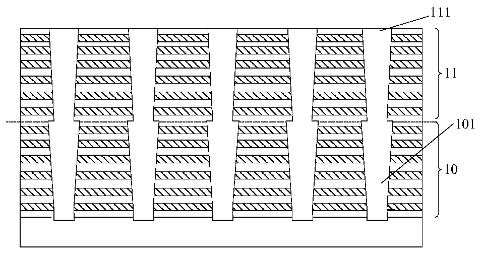
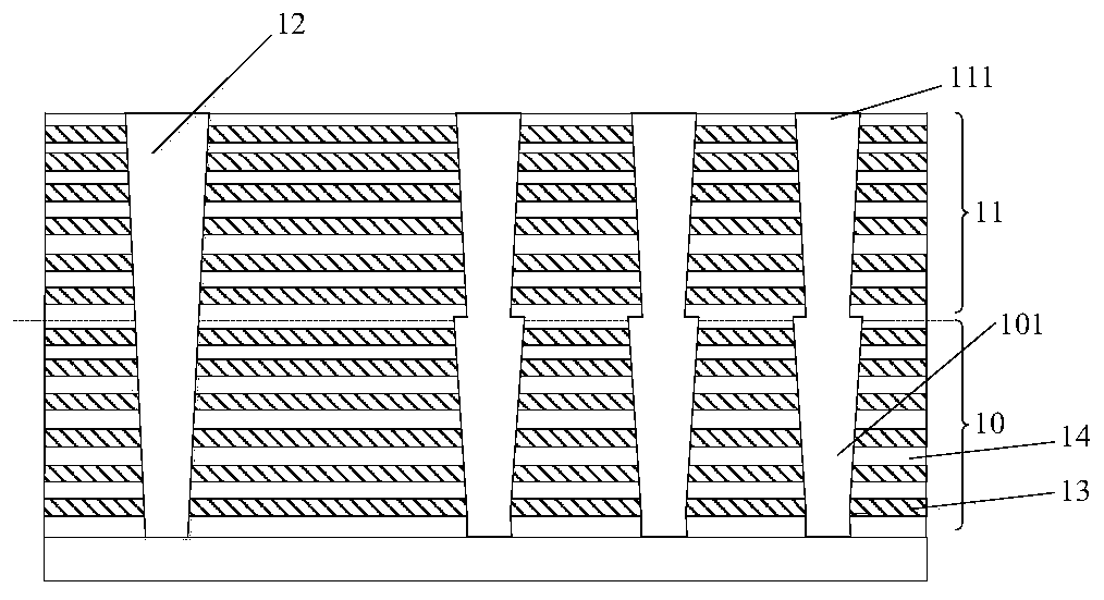
[0066] Based on the above-mentioned problems in the related art, the embodiment of the present application provides a method for forming a three-dimensional memory device, which adopts the method of separately etching channel holes and DCHs on the upper stack layer and the lower stack layer to form a double-layer three-dimensional memory device . While ensuring the upper channel hole and the lower channel hole of the double-layer three-dimensional memory device, the etching difficulty of the DCH is improved, and the etching depth of the DCH is reduced, thereby avoiding the problem of device defects and reducing the difficulty of the process.

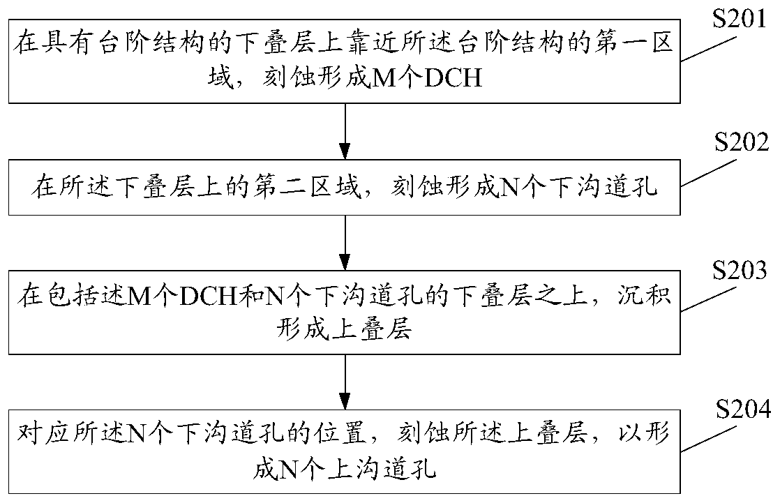
[0067] figure 2 It is a schematic flow diagram of a method for forming a three-dimensional storage device according to an embodiment of the present application, as shown in figure 2 As shown, the method includes the following steps:

[0068] Step S201 , forming M DCHs by etching in a first region close to the stepped structure on the...

Embodiment 2

[0091] An embodiment of the present application provides a method for forming a three-dimensional memory device, Figure 4 It is a schematic diagram of the implementation flow of another method for forming a three-dimensional storage device according to the embodiment of the present application, as shown in Figure 4 As shown, the method includes the following steps:

[0092] In step S401, the first material layer and the second material layer are stacked circularly on the substrate to form a lower stacked layer; the lower stacked layer is etched so that the lower stacked layer has a stepped structure.

[0093] Such as Figure 5A As shown, on the substrate 51 , after stacking the first material layer 501 and the second material layer 502 cyclically, the lower stacked layer is etched to form the lower stacked layer 52 with the stepped structure 521 .

[0094] Here, the substrate 51 is located at the lowest layer of the three-dimensional memory device, and the material of the ...

Embodiment 3

[0148] An embodiment of the present application provides a method for forming a three-dimensional memory device, Image 6 It is a schematic flow diagram of another method for forming a three-dimensional storage device in the embodiment of the present application, as shown in Image 6 As shown, the method includes the following steps:

[0149] In step S601 , according to a second preset stacking rule, the first material layer and the second material layer are stacked circularly on the substrate to form the lower stacked layer with a stepped structure.

[0150] Such as Figure 7A As shown, on the substrate 71 , the first material layer 701 and the second material layer 702 are stacked circularly to form the lower layer 72 with the stepped structure 721 .

[0151] Here, the second preset stacking rules include the following two types:

[0152] The first type, according to the same stacking pattern, the area of ​​each first material layer is larger than the area of ​​the first ...


PUM


Abstract

The embodiment of the invention discloses a forming method of a three-dimensional memory device, and the three-dimensional memory device, and the method comprises the steps: etching M DCHs in a firstregion on a lower lamination layer, wherein the lower lamination layer has a step structure, and the first area is close to the step structure; etching N lower channel holes in a second region on thelower lamination layer, wherein the second area is different from the first area, and M and N are positive integers; depositing to form an upper lamination layer on the lower lamination layer comprising the M DCHs and the N lower channel holes; and etching N upper channel holes in the upper lamination layer corresponding to the N lower channel holes in position.

Description

technical field [0001] Embodiments of the present invention relate to the field of semiconductor devices and their manufacture, and relate to, but are not limited to, a method for forming a three-dimensional storage device and a three-dimensional storage device. Background technique [0002] In order to overcome the limitations of two-dimensional memory devices, the industry has developed memory devices with a three-dimensional structure, and the integration density is increased by three-dimensionally arranging memory cells on a substrate. [0003] Existing double-layer three-dimensional memory devices, such as double-layer three-dimensional computer flash memory devices (3D NAND) memory devices, the upper stack and the lower stack are all vertically stacked with multi-layer memory cells of the same structure, using two layers of the same pattern The stacked layers are superimposed, thereby reducing the difficulty of etching deep channel holes (Channel Hole, CH), and adoptin...

Claims


Application Information

Patent Timeline
Patent Type & Authority Applications(China)
IPC IPC(8): H01L27/11582H01L27/11556
Inventor 姚兰
Owner YANGTZE MEMORY TECH CO LTD
Why Eureka
Try Eureka