Photoelectric memory based on two-dimensional heterojunction optical wavelength induction and preparation method thereof

A technology of optical wavelength and heterojunction, applied to semiconductor devices, circuits, electrical components, etc., can solve problems such as limited storage capacity, poor data storage capacity, and long data retention time, and achieve the goal of improving storage capacity and broad application prospects Effect

Inactive Publication Date: 2019-05-28
FUDAN UNIV
View PDF3 Cites 2 Cited by
  • Summary
  • Abstract
  • Description
  • Claims
  • Application Information

AI Technical Summary

Problems solved by technology

However, in past studies, optoelectronic memories fabricated with 2D materials have poor data storage capacity, with the highest reported data at about 8 different storage states, so the data storage capacity of optoelectronic memories based on 2D materials There is still a lot of room for improvement, a

Method used


Image

  • Photoelectric memory based on two-dimensional heterojunction optical wavelength induction and preparation method thereof
  • Photoelectric memory based on two-dimensional heterojunction optical wavelength induction and preparation method thereof
  • Photoelectric memory based on two-dimensional heterojunction optical wavelength induction and preparation method thereof

Examples


Embodiment Construction

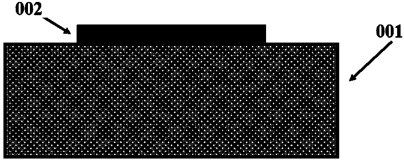
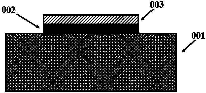
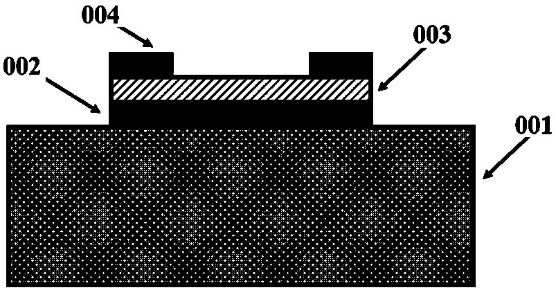
[0028] The following is a detailed description of the embodiments of the present invention. Examples of the embodiments are shown in the accompanying drawings, wherein the same or similar reference numerals indicate the same or similar materials or methods with the same or similar functions throughout. The embodiments described below with reference to the accompanying drawings are exemplary, and are only used to explain the present invention, and cannot be construed as limiting the present invention. In order to simplify the disclosure of the present invention, the materials and methods of specific examples are described below. Of course, they are only examples, and are not intended to limit the invention. In addition, the present invention provides examples of various specific processes and materials, but those of ordinary skill in the art may be aware of the applicability of other processes and / or the use of other materials.

[0029] Hereinafter, according to the attached draw...


PUM

PropertyMeasurementUnit
Thicknessaaaaaaaaaa
Thicknessaaaaaaaaaa
Thicknessaaaaaaaaaa

Abstract

The invention belongs to the technical field of photoelectric memories, and particularly relates to a nonvolatile photoelectric memory based on two-dimensional heterojunction optical wavelength induction and a preparation method thereof. According to the invention, different optical responses are generated on light with different wavelengths by using defect energy levels in a two-dimensional material, different charge storage states are realized under the driving of an electric field, and nonvolatile multi-value storage of the device is realized through bipolar change of a channel two-dimensional material and stepped change of the number of charges in a light absorption layer. The preparation method comprises the following steps: obtaining a two-dimensional material serving as a light absorption layer on a substrate by utilizing mechanical stripping or chemical vapor deposition, and then stacking the two-dimensional material with double polarities on the light absorption layer by utilizing a dry transfer technology to serve as a channel of a device. The novel nonvolatile photoelectric memory with the multi-value storage capability prepared by the invention has a wide application prospect in the field of future data photoelectric storage.

Description

Technical field [0001] The invention belongs to the technical field of photoelectric memory, and specifically relates to a non-volatile photoelectric memory induced by different light wavelengths based on a two-dimensional material heterojunction and a preparation method thereof. Background technique [0002] Photoelectric memory is a device that can store charge carriers under light conditions. These devices can be used in image capture and spectrum analysis systems. Two-dimensional atomic layered materials are good candidates for the development of next-generation optoelectronic memories to meet the emerging requirements of device miniaturization and flexibility. However, in the past research, the optoelectronic memory made of two-dimensional materials has poor data storage capacity, and has the highest report data in about 8 different storage states. Therefore, the data storage capacity of optoelectronic memory based on two-dimensional materials There is still a lot of room ...

Claims


Application Information

Patent Timeline
IPC IPC(8): H01L31/109H01L31/18
CPCY02P70/50
Inventor 张卫李家意王水源周鹏
Owner FUDAN UNIV
Why Eureka
Try Eureka