Unlock instant, AI-driven research and patent intelligence for your innovation.

Packaging substrate manufacturing process, packaging substrate and wafer packaging structure

A technology for packaging substrates and manufacturing processes, which is used in semiconductor/solid-state device manufacturing, electrical components, and electrical solid-state devices. The effect of market demand

Inactive Publication Date: 2019-06-04
SHENZHEN ZHIJIN ELECTRONICS
View PDF3 Cites 1 Cited by
  • Summary
  • Abstract
  • Description
  • Claims
  • Application Information

AI Technical Summary

Problems solved by technology

[0003] In order to overcome the deficiencies of the prior art, one of the purposes of the present invention discloses a packaging substrate manufacturing process, which is used to solve the problem that the existing packaging structure of the existing wafer makes the product overall thicker and cannot meet the market demand.

Method used


Image

  • Packaging substrate manufacturing process, packaging substrate and wafer packaging structure
  • Packaging substrate manufacturing process, packaging substrate and wafer packaging structure
  • Packaging substrate manufacturing process, packaging substrate and wafer packaging structure

Examples


Embodiment Construction

[0041] Below, the present invention will be further described in conjunction with the accompanying drawings and specific implementation methods. It should be noted that, under the premise of not conflicting, the various embodiments described below or the technical features can be combined arbitrarily to form new embodiments. .

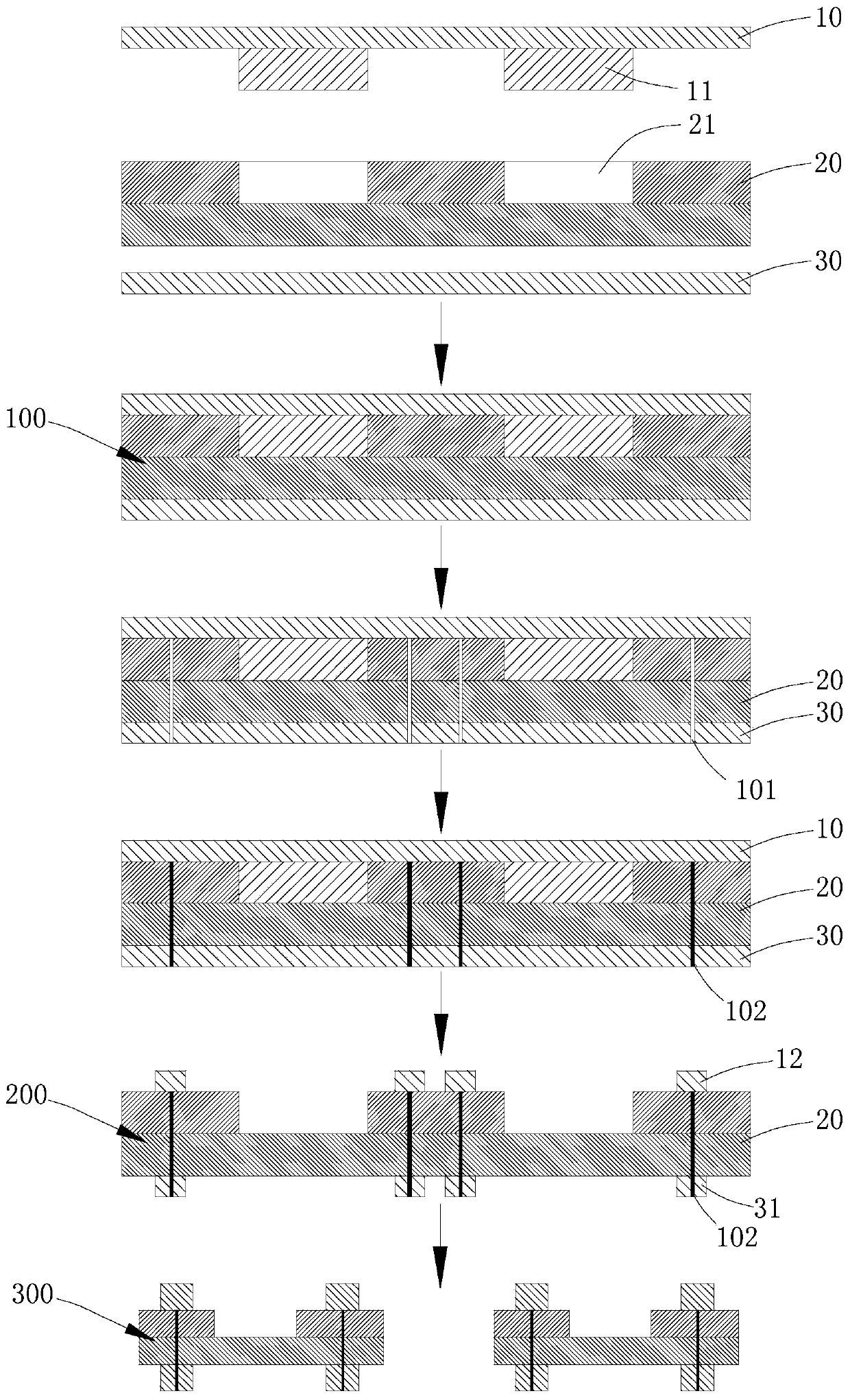
[0042] see Figure 1-2 , a packaging substrate manufacturing process S100 disclosed in an embodiment of the present invention is used to manufacture a packaging substrate for wafer packaging. The packaging substrate manufacturing process S100 includes:

[0043] In step S10, the first conductive sheet 10 with the boss 11 on one side and the insulator 20 with the receiving cavity 21 on one side are stacked and pressed together in such a way that the boss 11 is opposite to the receiving cavity 21, and the boss 11 is accommodated in the In the housing cavity 21, the second conductive sheet 30 is stacked and pressed on the side of the insulating member 20 ...


PUM

PropertyMeasurementUnit
Thicknessaaaaaaaaaa

Abstract

The invention discloses a packaging substrate manufacturing process, a packaging substrate and a wafer packaging structure. The packaging substrate manufacturing process comprises the steps of: laminating a first conductive piece, an insulator and a second conductive piece to form a base material; processing the first conductive piece, the insulator and the second conductive piece to form lead wires, first wiring projections connected with one ends of the lead wires, and second wiring projections connected with the other ends of the lead wires; and removing bosses to expose accommodating cavities. Therefore, the packaging substrate having a packaging circuit and the accommodating cavities allowing wafers to embed and package can be formed in one step by adopting the packaging substrate manufacturing process, the process is simple, the cost is low, the packaging substrate can be manufactured in batch, the production efficiency is high, and the wafers can be embedded and packaged in thepackaging substrate manufactured by adopting the packaging substrate manufacturing process, thus the overall thickness of the product is thin, and the market demand can be met.

Description

technical field [0001] The invention relates to the field of wafer packaging, in particular to a manufacturing process of a packaging substrate, a packaging substrate and a wafer packaging structure using the packaging substrate. Background technique [0002] Existing integrated circuit packaging substrates are all planar structures. During wafer packaging, the wafer is directly attached to the surface of the packaging substrate. With the development of refined and thinner products, the existing wafer packaging structure makes the overall product relatively Thick, can not meet the needs of the market. Contents of the invention [0003] In order to overcome the deficiencies of the prior art, one of the objectives of the present invention is to disclose a packaging substrate manufacturing process, which is used to solve the problem that the existing packaging structure of the existing wafer makes the product overall thicker and cannot meet the market demand. The second obje...

Claims


Application Information

Patent Timeline
IPC IPC(8): H01L21/48H01L23/498
CPCH01L2224/48091H01L2924/15153H01L2924/00014
Inventor 康孝恒蔡克林倪超李瑞邱龙洲许凯
Owner SHENZHEN ZHIJIN ELECTRONICS
Features
  • R&D
  • Intellectual Property
  • Life Sciences
  • Materials
  • Tech Scout
  • Unparalleled Data Quality
  • Higher Quality Content
  • 60% Fewer Hallucinations
Learn More