Packaging body for reducing lamination packaging structure of communication chip

A communication chip and stacked package technology, which is applied in the package field of communication chips with reduced stacked package structure, can solve the problems of limited heat dissipation effect, achieve the effects of increasing heat dissipation channels, improving heat dissipation efficiency, and improving air tightness

Inactive Publication Date: 2019-06-07
南京双电科技实业有限公司
View PDF7 Cites 2 Cited by
  • Summary
  • Abstract
  • Description
  • Claims
  • Application Information

AI Technical Summary

Problems solved by technology

[0004] The purpose of the present invention is to provide a package for communication chips with a reduced stacked packaging structure, so as to solve the problem that the heat dissipation effect of the existing communication chip packages proposed in the above background technology is limited, and an external cooling fan is often required to ensure long-term operation. The problem

Method used


Image

  • Packaging body for reducing lamination packaging structure of communication chip
  • Packaging body for reducing lamination packaging structure of communication chip
  • Packaging body for reducing lamination packaging structure of communication chip

Examples


Embodiment Construction

[0026] The following will clearly and completely describe the technical solutions in the embodiments of the present invention with reference to the accompanying drawings in the embodiments of the present invention. Obviously, the described embodiments are only some, not all, embodiments of the present invention.

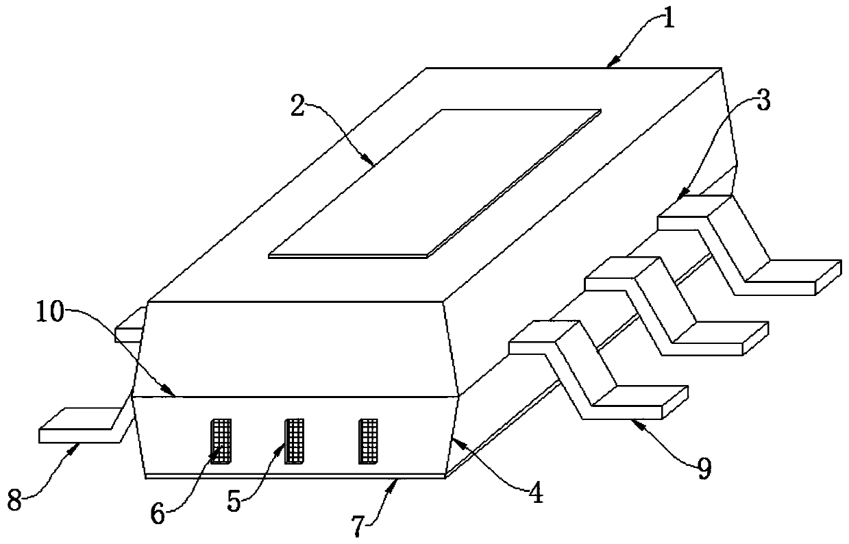
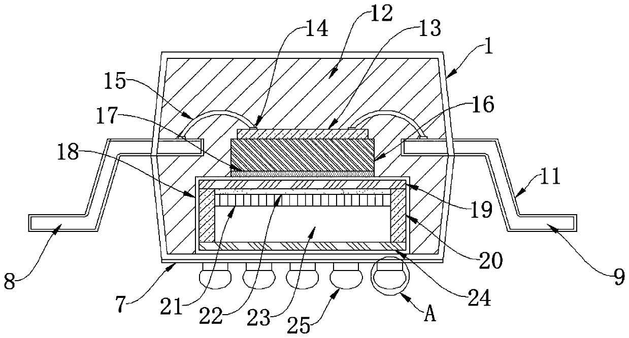
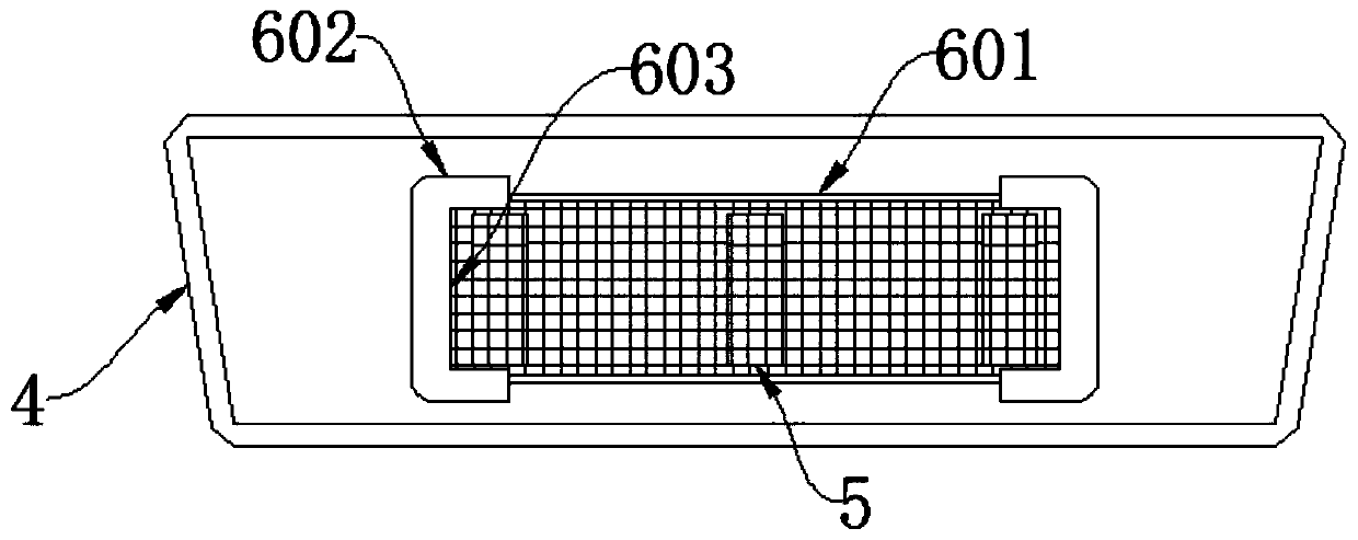
[0027] see Figure 1-5 , an embodiment provided by the present invention: a package body for reducing the stacked packaging structure of communication chips, including an upper insulating shell 1, and a model label 2 is arranged on the upper surface of the upper insulating shell 1, and the model label 2 can be conveniently The specifications of the communication chip are identified, and one side of the upper insulating shell 1 is provided with an input pin 8, which can introduce the current in the circuit board, and the other side of the upper insulating shell 1 is provided with an output pin 9, The output pin 9 can lead the current inside the communication chip 13 b...


PUM


Abstract

The invention discloses a packaging body for reducing a lamination packaging structure of a communication chip, which relates to the technical field of packaging bodies. In order to solve the problemthat the heat dissipation effects of the existing communication chip packaging body are limited, an external heat dissipation fan is often required to be connected to ensure long-time operation. The upper surface of an upper insulating case is provided with a model label, one side of the upper insulating case is provided with an input pin, the other side of the upper insulating case is provided with an output pin, the outer walls of the input pin and the output pin are both provided with metal coatings; the outer walls of two sides of the upper insulating case are provided with pin grooves, one end of the input pin and one end of the output pin pass to extend to the inner parts of the pin grooves, a lower insulating case is arranged below the upper insulating case, a welding plate is arranged on the lower surface of the lower insulating case, the welding plate is internally provided with a connection notch, and a welding ball is arranged below the connection notch.

Description

technical field [0001] The invention relates to the technical field of packaging bodies, in particular to a packaging body used for reducing stacked packaging structures of communication chips. Background technique [0002] The so-called "packaging technology" is a technology of packaging integrated circuits with insulating plastic or ceramic materials. Taking the CPU as an example, the actual size and appearance are not the size and appearance of the real CPU core, but the packaged products of the CPU core and other components. Packaging technology is necessary and crucial for chips. , because the chip must be isolated from the outside world to prevent impurities in the air from corroding the chip circuit and causing electrical performance degradation. On the other hand, the packaged chip is also easier to install and transport. Since the quality of packaging technology also directly affects the performance of the chip itself and the design and manufacture of the PCB conne...

Claims


Application Information

Patent Timeline
Patent Type & Authority Applications(China)
IPC IPC(8): H01L23/367H01L23/467H01L23/057
CPCH01L2224/48247H01L2224/73265H01L2924/181H01L2924/00012
Inventor 卢俊
Owner 南京双电科技实业有限公司
Why Eureka
Try Eureka