Display panel and display device
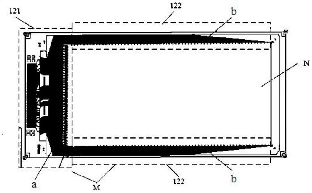
A display panel and display layer technology, which is applied to semiconductor devices, electrical components, circuits, etc., can solve the problem that the display panel cannot achieve a borderless design.
- Summary
- Abstract
- Description
- Claims
- Application Information
AI Technical Summary
Problems solved by technology
Method used
Image
Examples
Embodiment 1
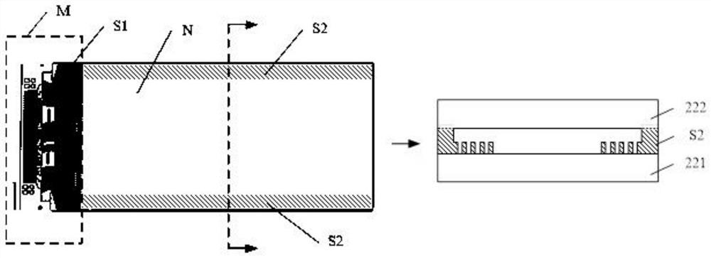
[0035] In this embodiment, a display panel is provided, which is used to improve the problem that the existing output leads are routed in the frame area of the display panel and the display panel cannot realize a frameless design, figure 2 It is a schematic diagram of the structure of the display panel in this solution. The left part of the figure is a top view of the display panel, and the right part is a schematic cross-sectional structure diagram obtained by cutting along the dotted line in the display panel corresponding to the left figure. The display panel includes: a substrate 221, a display layer 222 located on the substrate 221; the display panel defines a display area N corresponding to the display layer 222 and a non-display area M including at least a bonding area; For at least one edge area of the display area N connected with the output lead S2: the output lead S2 is arranged between the substrate 221 and the display layer 222, and the output lead S2 is on th...
Embodiment 2
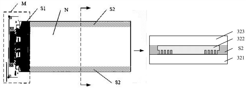
[0043] Based on the display panel structure of the above-mentioned embodiment, the embodiment of the present invention also provides a better display panel, which is used to improve the problem that the existing output leads are laid in the frame area of the display panel, which restricts the display panel from being unable to achieve a frameless design. FIG. 3 is a schematic diagram of the structure of the display panel of this solution.
[0044] In the display panel structure of this embodiment, in the wiring area of the output lead S2 other than the connection point between the output lead S2 and the display layer 323, a first insulating layer is arranged between the output lead S2 and the display layer. 322.
[0045] The material of the insulating layer can be polymer insulating material such as polyethylene, or rubber or organic glue. In the actual production process, affected by the production process, the insulating layer can be made of an inorganic material with s...
Embodiment 3
[0066] In this embodiment, a display device is provided, which is used to solve the problem in the prior art that a display panel needs to be provided with a frame due to the routing of output leads through a frame position, and the device includes any display panel in the above embodiments.
[0067] Based on the display panel structures of the above embodiments, the display device provided by this embodiment can realize a frameless structure on at least one edge connected with output leads. Taking a rectangular display device as an example, this solution can optimally realize a three-sided borderless structure, thereby increasing the screen-to-body ratio of the display device and improving visual experience. In addition, in addition to the display panel, the device may also include a polarizer, a filter, a protective film, etc., to improve the overall display performance of the display device or prolong the service life of the device.
PUM
 Abstract
Description
Claims
Application Information


