
Chip package structure and manufacturing method thereof

A technology of chip packaging and manufacturing methods, applied in semiconductor/solid-state device manufacturing, electrical components, electric solid-state devices, etc., can solve the problems of occupying space, space waste of the lead frame 100, and design restrictions of the lead frame 100, and achieve effective utilization , to avoid restrictive effects

Inactive Publication Date: 2007-07-18
ADVANCED SEMICON ENG INC
View PDF0 Cites 0 Cited by
  • Summary
  • Abstract
  • Description
  • Claims
  • Application Information

AI Technical Summary

Problems solved by technology

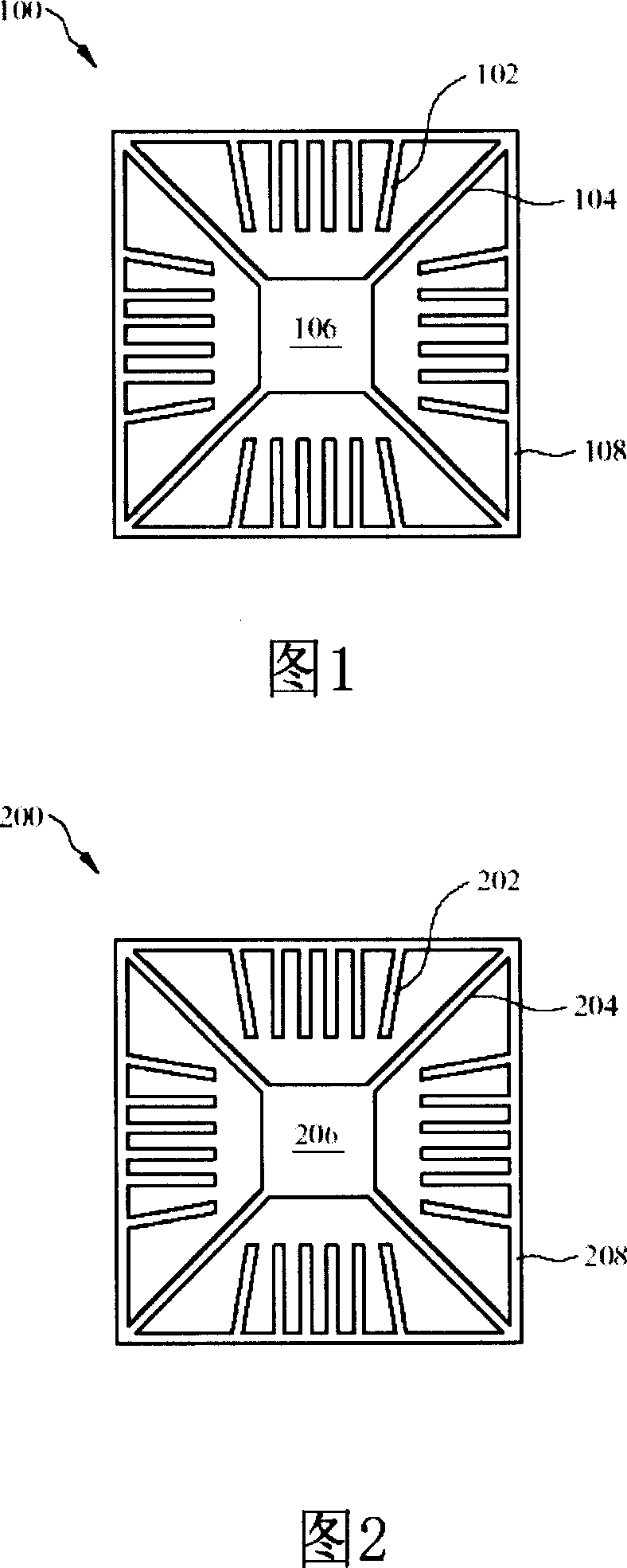
[0005] However, the existence of these support bars 104 occupies the space of the four corners of the lead frame 100, so that the guide pins 102 cannot be arranged at the four corners of the lead frame 100, which not only wastes the space of the lead frame 100, but also affects the wires. The architectural design of the rack 100 poses limitations

Method used


Image

  • Chip package structure and manufacturing method thereof
  • Chip package structure and manufacturing method thereof
  • Chip package structure and manufacturing method thereof

Examples


Embodiment Construction

[0017] Relevant detailed description and technical contents of the present invention are as follows now in conjunction with the accompanying drawings:

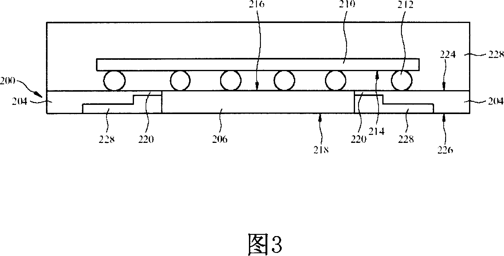
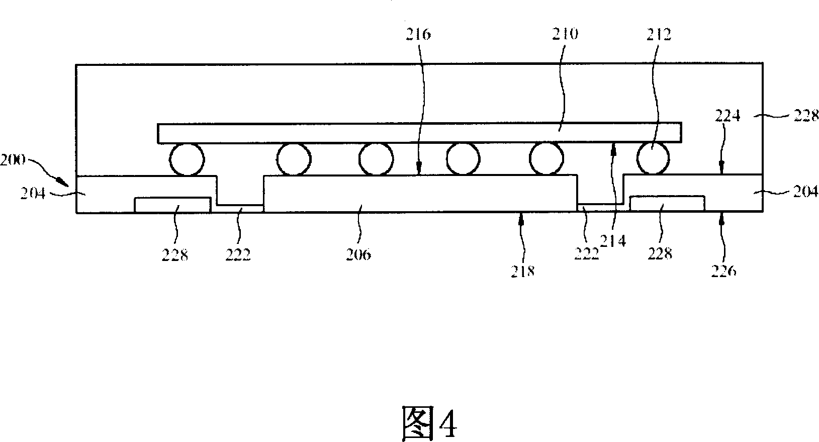
[0018] The invention discloses a chip package structure and a manufacturing method thereof. The chip package structure is a four-sided flat package structure without leads. In order to make the description of the present invention more detailed and complete, reference may be made to the following description together with the illustrations in FIGS. 2 to 4 .

[0019] Please refer to FIGS. 2 to 4 , wherein FIG. 2 is a top view of a lead frame according to a preferred embodiment of the present invention, and FIGS. 3 and 4 are two different chip packaging structures according to a preferred embodiment of the present invention. sectional view. The chip packaging structure of the present invention has a carrier, such as a lead frame 200 , whose main function is to carry a chip 210 , as shown in FIGS. 3 and 4 . In the chip packagin...


PUM


Abstract

The invention relates to one kind of a chip package structure and its manufacturing methods. The chip package structure at least includes a loader device and a chip configured on the loader. The loader at least includes a radiation pad with a bearing surface, some guiding feet and at least two biramous bracings. In addition, the above chip includes a number of solder balls polycrystalline-interfaced with the radiation pad, the guiding feet and the biramous bracings of the loader.

Description

technical field [0001] The present invention relates to a chip packaging structure and a manufacturing method thereof, and in particular to a quad flat no-lead (QFN) packaging structure and a manufacturing method thereof. Background technique [0002] With the increasing integration of integrated circuits and the demand for high-performance electronic products, packaging technology is driven to develop in the direction of increasing packaging density, reducing package size, and shortening transmission distance to meet the size reduction of integrated circuit components. and the trend of continuous growth of input / output (Input / Output; I / O) numbers. [0003] There are many types of packaging for integrated circuits, and a very common packaging type is to provide a lead frame first, wherein the lead frame has a chip holder and a plurality of leads disposed on the periphery of the chip holder. Next, the chip is attached to the chip holder and the peripheral pins by using the s...

Claims


Application Information

Patent Timeline
Patent Type & Authority Applications(China)
IPC IPC(8): H01L23/488H01L21/60
CPCH01L2224/16245
Inventor 刘千王盟仁
Owner ADVANCED SEMICON ENG INC
Learn More