Preparation method of light-emitting panel, light-emitting panel and display device

A technology for light-emitting panels and light-emitting devices, which is used in the manufacture of semiconductor/solid-state devices, electrical components, and electrical solid-state devices. question

Inactive Publication Date: 2019-06-11
WUHAN CHINA STAR OPTOELECTRONICS SEMICON DISPLAY TECH CO LTD
View PDF7 Cites 2 Cited by
  • Summary
  • Abstract
  • Description
  • Claims
  • Application Information

AI Technical Summary

Problems solved by technology

[0003] In the prior art, in order to prevent water and oxygen from infiltrating from the side of the display device, a hydrophobic retaining wall or a raised retaining wall is generally arranged between two inorganic packaging layers, so that water and oxygen cannot penetrate into the device, but because the retaining wall is If

Method used


Image

  • Preparation method of light-emitting panel, light-emitting panel and display device
  • Preparation method of light-emitting panel, light-emitting panel and display device
  • Preparation method of light-emitting panel, light-emitting panel and display device

Examples


Embodiment Construction

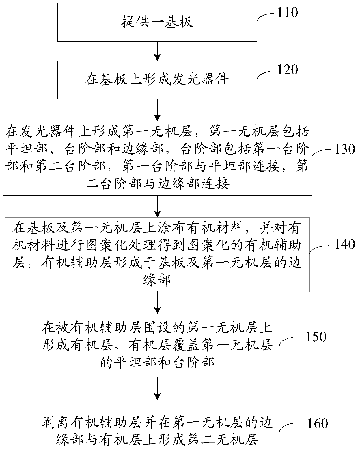
[0040] The technical solutions in the embodiments of the present application will be clearly and completely described below in conjunction with the drawings in the embodiments of the present application. Apparently, the described embodiments are only some of the embodiments of this application, not all of them. Based on the embodiments in this application, all other embodiments obtained by those skilled in the art without making creative efforts belong to the scope of protection of this application.

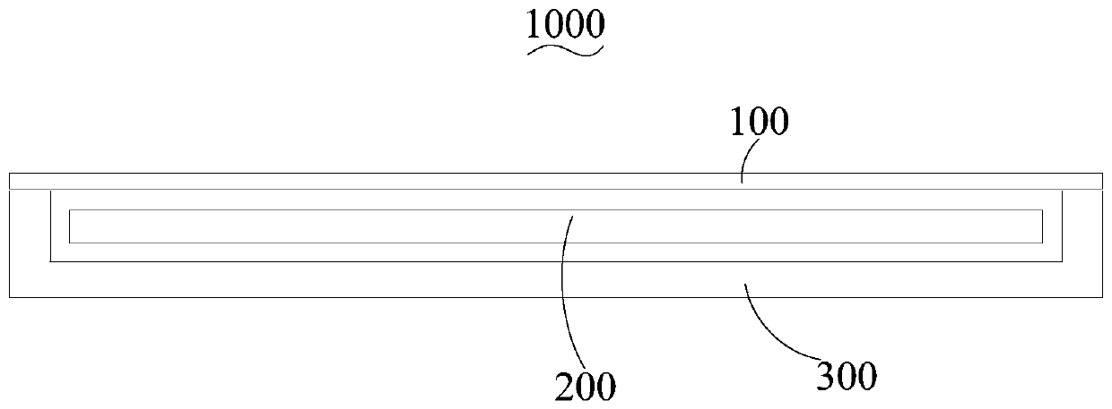
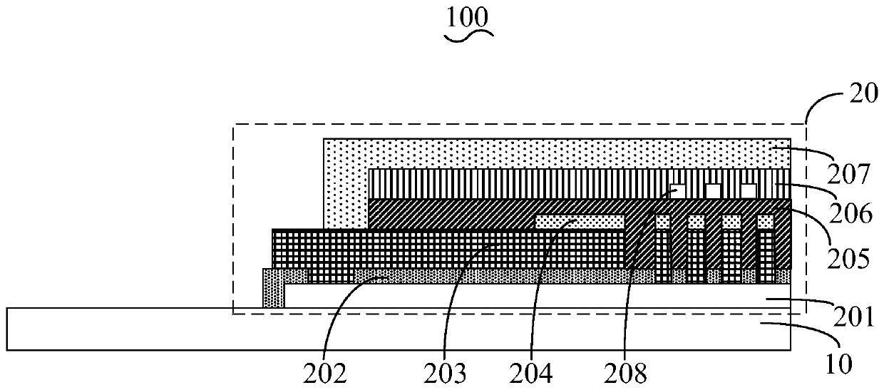
[0041] With the gradual maturity of organic light emitting device (Organic Light Emitting Diode, OLED) technology, higher and higher requirements have been put forward for the reliability of OLED. In terms of reliability, the intrusion of water and oxygen from the side of the encapsulation layer is a major challenge. , and this challenge mainly comes from two aspects. First, the characteristics of the film layer change when the encapsulation layer and the array substrate are in a...


PUM


Abstract

The invention discloses a preparation method of a light-emitting panel, the light-emitting panel and a display device; the preparation method comprises the steps that a substrate is provided; a light-emitting device is formed on the substrate; a first inorganic layer is formed on the light-emitting device, wherein the first inorganic layer comprises a flat part, a step part and an edge part; the step part comprises a first step part and a second step part; the first step part is connected with the flat part, and the second step part is connected with the edge part; the substrate and the firstinorganic layer are coated with organic materials, and patterning is carried out on the organic materials to obtain the patterned organic auxiliary layer, wherein the organic auxiliary layer is formedon the edge parts of the substrate and the first inorganic layer; an organic layer is formed on the first inorganic layer which is surrounded by the organic auxiliary layer, and the organic layer covers the flat part and the step part of the first inorganic layer; and the organic auxiliary layer is stripped off, and a second inorganic layer is formed on the edge parts of the first inorganic layerand the organic layer, so that the arrangement of a retaining wall is avoided, thereby lowering the possibility of stripping between the film layers.

Description

technical field [0001] The present application relates to the field of display technology, in particular to a method for preparing a light-emitting panel, a light-emitting panel and a display device. Background technique [0002] In recent years, organic light emitting devices (Organic Light Emitting Diode, OLED) have become the most promising new display devices in recent years due to their advantages such as self-luminescence, all-solid-state, and high contrast. With the continuous improvement of users' requirements on the quality of display devices, packaging technology is particularly critical. [0003] In the prior art, in order to prevent water and oxygen from penetrating from the side of the display device, a hydrophobic retaining wall or a raised retaining wall is generally arranged between two inorganic packaging layers, so that water and oxygen cannot penetrate into the device, but because the retaining wall is If it is placed between two inorganic encapsulation l...

Claims


Application Information

Patent Timeline
IPC IPC(8): H01L27/32H01L51/52H01L51/56
Inventor 金江江
Owner WUHAN CHINA STAR OPTOELECTRONICS SEMICON DISPLAY TECH CO LTD
Why Eureka
Try Eureka