A pcb ink curing device

A curing device and ink technology, which is applied to printing devices, typewriters, printing, etc., can solve problems such as increased production costs, uneven inkjet, PCB board damage, etc., and achieve the effect of convenient and precise inkjet, stable and fast delivery

Active Publication Date: 2020-11-17
ICHIA TECH SUZHOU
View PDF9 Cites 0 Cited by
  • Summary
  • Abstract
  • Description
  • Claims
  • Application Information

AI Technical Summary

Problems solved by technology

[0004] The purpose of the present invention is to provide a PCB ink curing device. In order to overcome the above-mentioned existing PCB board during the production process, the inkjet curing process of the PCB board cannot be realized. Fully automatic integrated operation requires manual cooperation to complete the PCB. PCB production, and during the inkjet curing process of PCB boards, damage to the PCB board and uneven inkjet phenomenon are prone to occur, which affects the production efficiency of the PCB board, and the rate of defective products is high, resulting in an increase in production costs. question

Method used


Image

  • A pcb ink curing device
  • A pcb ink curing device
  • A pcb ink curing device

Examples


Embodiment Construction

[0039] The technical solutions of the present invention will be clearly and completely described below in conjunction with the embodiments. Apparently, the described embodiments are only some of the embodiments of the present invention, not all of them. Based on the embodiments of the present invention, all other embodiments obtained by persons of ordinary skill in the art without creative efforts fall within the protection scope of the present invention.

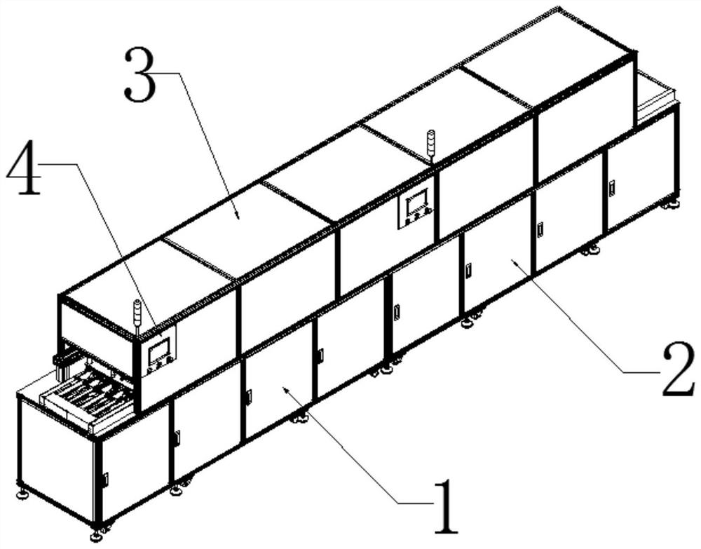
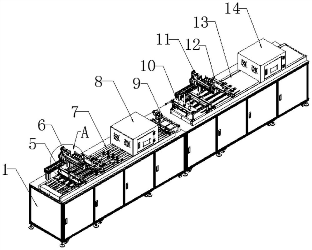
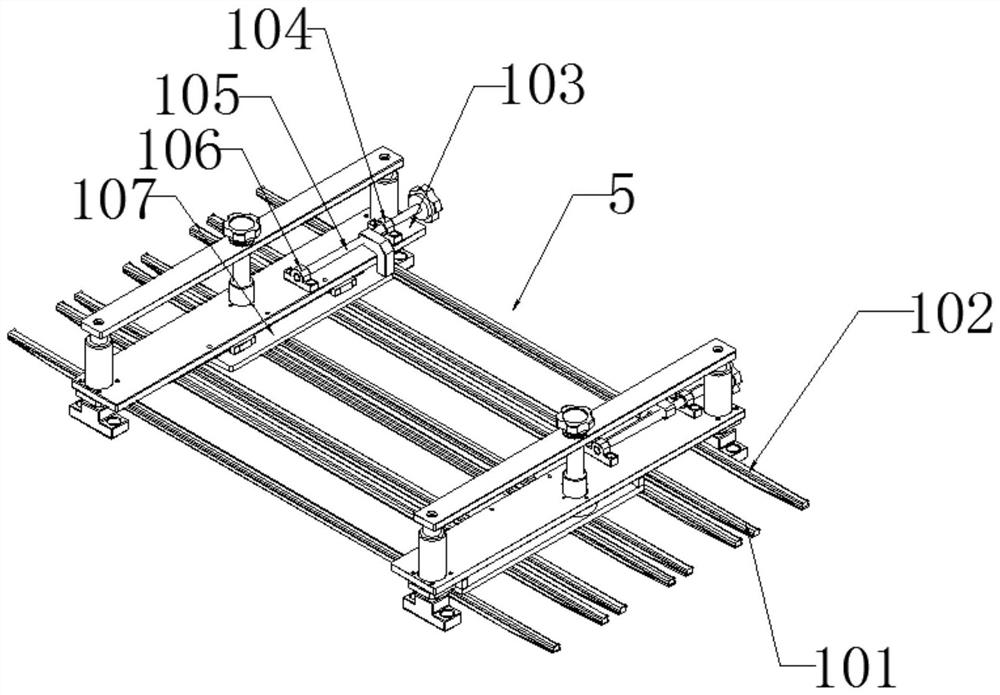
[0040] see Figure 1-10 As shown, a PCB ink curing device includes a first frame 1, a second frame 2, a first positioning mechanism 5, a first inkjet mechanism 6, a first conveyor belt 7, a first curing box 8, and a turning mechanism 9 , feeding mechanism 10, the second inkjet mechanism 11, the second positioning mechanism 12, the second conveyor belt 13 and the second curing box 14, the first frame 1 side is equipped with the second frame 2, the first frame 1 top The first conveyor belt 7 is installed, the first positioni...


PUM


Abstract

The invention discloses a PCB printing ink curing device. The PCB printing ink curing device comprises a first rack, a second rack, a second conveyor belt and a second curing box, wherein the second rack is mounted at one side of the first rack; a first conveyor belt is mounted on the top of the first rack; a first positioning mechanism, a first curing box and a turnover mechanism are sequentiallymounted on positions, above the first conveyor belt, on the top of the first rack; a first ink-jet mechanism is positioned on the middle position above the first positioning mechanism; the bottom ofthe first ink-jet mechanism is fixedly arranged at one side above the first rack; and a second conveyor belt is mounted on the top of the second rack. The PCB printing ink curing device performs an ink-jet curing processing process on a PCB, realizes fully-automatic integrated operation, and does not need to manually cooperate to accomplish PCB production; and moreover, in an ink-jet curing processing process of the PCB, a low damage rate and uniform ink-jet curing of the PCB can be guaranteed, production efficiency of the PCB is guaranteed, and production cost of the PCB is reduced.

Description

technical field [0001] The invention relates to the field of PCB board production devices, in particular to a PCB ink curing device. Background technique [0002] PCB board is also called printed circuit board, printed circuit board, referred to as printed board, with insulating board as the base material, cut to a certain size, with at least one conductive pattern attached to it, and holes (such as component holes, fastening holes) , metallized holes, etc.), used to replace the chassis of the previous installation of electronic components, and to realize the interconnection between electronic components. Because this kind of board is made by electronic printing, it is called "printed" circuit board. It is not accurate to call "printed circuit board" as "printed circuit" because there is no "printed circuit board" on the printed board. Printed components" and only wiring; PCB boards need to be inkjet on the copper clad board and then cured during the production process. ...

Claims


Application Information

Patent Timeline
Patent Type & Authority Patents(China)
IPC IPC(8): B41J11/00B41J2/01B41J3/407
Inventor 林少慧金会兰
Owner ICHIA TECH SUZHOU
Why Eureka
Try Eureka