Array substrate, display panel and display device
An array substrate and substrate technology, applied in the field of display panels, display devices, and array substrates, can solve the problems affecting the display performance of flexible display devices, film cracking, dislocation, etc., and achieve the effect of ensuring normal display and preventing corrosion.
- Summary
- Abstract
- Description
- Claims
- Application Information
AI Technical Summary
Problems solved by technology
Method used
Image

Examples
Embodiment Construction
[0023] The present invention will be further described in detail below in conjunction with the accompanying drawings and embodiments. It should be understood that the specific embodiments described here are only used to explain the present invention, but not to limit the present invention. In addition, it should be noted that, for the convenience of description, only some structures related to the present invention are shown in the drawings but not all structures.
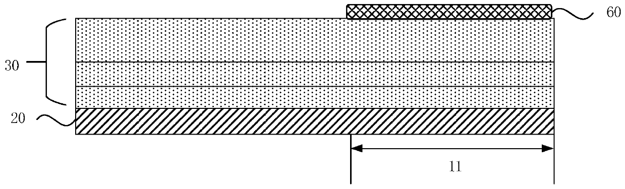
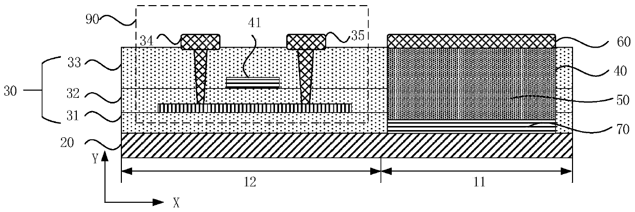
[0024] figure 1 is a schematic structural diagram of an array substrate in the prior art, such as figure 1 As shown, the array substrate includes a bending area 11, and also includes a flexible substrate 20, an inorganic insulating layer 30, and a metal wiring 60. When the array substrate is bent, the bending area 11 will bear excessively concentrated stress. The inorganic insulating layer 30 in the folding region 11 has a high hardness, so that the stress in the array substrate cannot be released, resulting in p...
PUM
 Abstract
Description
Claims
Application Information