Display panel and preparation method thereof

A technology for display panels and backplanes, which is applied to electrical components, electrical solid-state devices, circuits, etc., and can solve the problems of difficult process implementation and large seams

Active Publication Date: 2019-06-14
BOE TECH GRP CO LTD +1
View PDF4 Cites 13 Cited by
  • Summary
  • Abstract
  • Description
  • Claims
  • Application Information

AI Technical Summary

Problems solved by technology

[0005] The technical problem to be solved by the embodiments of the present invention is to provide a display panel and its prepar

Method used


Image

  • Display panel and preparation method thereof
  • Display panel and preparation method thereof
  • Display panel and preparation method thereof

Examples


no. 1 example

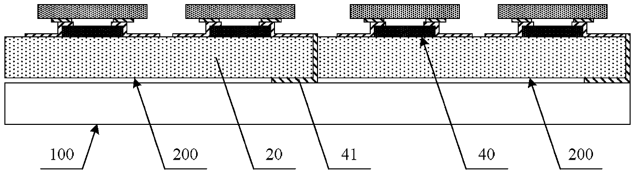
[0075] figure 2 It is a schematic structural diagram of the first embodiment of the display panel of the present invention, and the display panel is an active driving type. Such as figure 2 As shown, the main structure of the display panel in this embodiment includes a motherboard 100 and a plurality of backplanes 200 . Wherein, the motherboard 100 includes a motherboard substrate and a plurality of driving leads 11 arranged on the motherboard substrate, and each backplane 200 includes a backplane substrate and an extraction electrode 30 and a light emitting unit 40 arranged on the backplane substrate, and the light emitting unit 40 includes a driving circuit and a light-emitting diode. The light-emitting diode is a top emission structure. The light emitted by the light-emitting diode is emitted from the side of the motherboard 100, that is, the motherboard 100 serves as the display surface of the display panel.

[0076] Wherein, the plurality of backplanes 200 are arrange...

no. 2 example

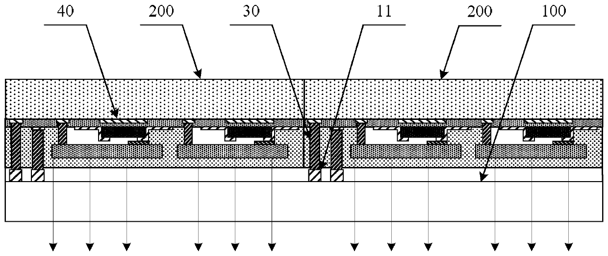
[0096] Figure 8 It is a schematic structural diagram of the second embodiment of the display panel of the present invention. The display panel is an active driving type, which is an extension based on the aforementioned first embodiment. Such as Figure 8 As shown, the main structure of the display panel of this embodiment is the same as that of the aforementioned first embodiment, including a motherboard 100 and a plurality of backplanes 200, and the plurality of backplanes 200 are set up against each other and bound to the motherboard 100 in a flip-chip manner. , the motherboard 100 includes a motherboard substrate and a plurality of drive leads 11 arranged on the motherboard substrate, each backplane 200 includes a backplane substrate and an extraction electrode 30 and a light emitting unit 40 arranged on the backplane substrate, the light emitting unit 40 Including drive circuit and light emitting diode. Different from the aforementioned first embodiment, the light-emit...

no. 3 example

[0111] Based on the technical ideas of the foregoing embodiments, the embodiments of the present invention also provide a method for manufacturing a display panel. The preparation method of the display panel in this embodiment includes:

[0112] S1. Prepare a motherboard provided with driving leads, and prepare a plurality of backplanes provided with lead-out electrodes and light-emitting units;

[0113] S2. Bind the plurality of backplanes to the motherboard so that they are adjacent to each other, and the surface on the side of the backplane on which the lead-out electrodes and the light-emitting unit are set faces the surface on the side of the motherboard on which the driving leads are set, so The lead-out electrodes on the backboard are connected to the driving leads on the motherboard.

[0114] Wherein, preparing the motherboard provided with the driving leads in step S1 includes: forming the driving leads on the motherboard substrate; or forming a reflective layer or a...


PUM


Abstract

Embodiments of the invention provide a display panel and a preparation method thereof. The display panel comprises a mother board and a plurality of back boards which are mutually arranged and bound on the mother board; a driving lead is arranged on the mother board; a leading-out electrode and a light-emitting unit are arranged on each back board; the surface of one side, provided with the leading-out electrode and the light-emitting unit, of the back board faces the surface of one side, provide with the driving lead, of the mother board; and the leading-out electrodes on the back boards areconnected with the driving lead on the mother board. According to the display panel, the driving lead is arranged on the mother board, the leading-out electrode is arranged on each back board, and theplurality of back boards are inversely arranged on the mother board, and the leading-out electrodes are connected with the driving lead, so that the phenomenon that a leading-out wire or a through hole penetrating through the back board is arranged on the side edge of the back board or behind the back plate is avoided, the distance between the adjacent back boards is reduced to the largest extent, the non-mature side edge leading wire process and the double-sided process are also avoided, and the process implementation difficulty is reduced to the maximum extent.

Description

technical field [0001] The invention relates to the field of display technology, in particular to a display panel and a preparation method thereof. Background technique [0002] Semiconductor light-emitting diode (Light Emitting Diode, LED) technology has been developed for nearly three decades, from the initial solid-state lighting power supply to the backlight source in the display field and then to the LED display screen, providing a solid foundation for its wider application. Among them, with the development of chip manufacturing and packaging technology, sub-millimeter light-emitting diode (Mini Light Emitting Diode, Mini LED) display and micro light-emitting diode (Micro Light Emitting Diode, Micro LED) display have gradually become a hot spot for display panels. Micro LED Displays are mainly used in AR / VR and other fields, and Mini LED displays are mainly used in TV and outdoor display applications. [0003] Although the current display market is dominated by liquid ...

Claims


Application Information

Patent Timeline
IPC IPC(8): H01L33/62H01L25/075
Inventor 曲连杰齐永莲张珊赵合彬杨瑞智徐晓玲贾宁
Owner BOE TECH GRP CO LTD
Why Eureka
Try Eureka