Check patentability & draft patents in minutes with Patsnap Eureka AI!

Method and transfer tool for transferring semiconductor chips

A semiconductor and chip technology, applied in the direction of semiconductor devices, semiconductor/solid-state device manufacturing, semiconductor/solid-state device components, etc., can solve time-consuming and other problems

Active Publication Date: 2021-09-24
OSRAM OPTO SEMICON GMBH & CO OHG
View PDF7 Cites 0 Cited by
  • Summary
  • Abstract
  • Description
  • Claims
  • Application Information

AI Technical Summary

Problems solved by technology

This is associated with a considerable expenditure of time, especially when producing devices with a plurality of semiconductor chips

Method used


Image

  • Method and transfer tool for transferring semiconductor chips
  • Method and transfer tool for transferring semiconductor chips
  • Method and transfer tool for transferring semiconductor chips

Examples


Embodiment Construction

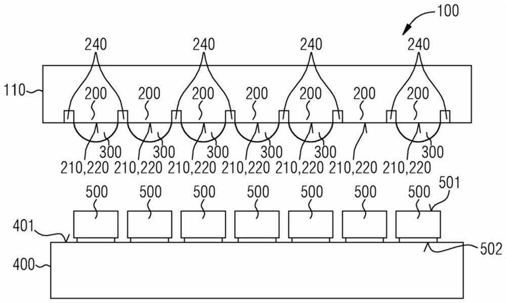
[0080] figure 1 A cutaway schematic side view of a portion of transfer tool 100 is shown. The transfer tool 100 is provided for transferring semiconductor chips selectively and in parallel from a source carrier to a target carrier. The transfer tool 100 here enables simultaneous and parallel transfer of a plurality of semiconductor chips. Furthermore, the transfer tool 100 makes it possible not to transfer all semiconductor chips present on the source carrier, but to selectively select the semiconductor chips to be transferred.

[0081] also, figure 1 A cutaway schematic side view of a portion of source carrier 400 is shown. A semiconductor chip 500 is arranged on the upper side 401 of the source carrier 400 . The semiconductor chips 500 may be present in a regular one-dimensional or two-dimensional arrangement, for example in a two-dimensional matrix arrangement. In this case, all grid positions of the regular arrangement can be occupied by the semiconductor chip 500 . ...


PUM

PropertyMeasurementUnit
bond strengthaaaaaaaaaa
thicknessaaaaaaaaaa

Abstract

A method for transferring semiconductor chips, said method comprising the steps of: providing a transfer tool having a plurality of sections, wherein each section has a liquid receiving area; in a regular arrangement on a source carrier providing a plurality of semiconductor chips; providing a target carrier; selectively disposing liquid droplets on the liquid containing areas of at least some of the segments; bringing the transfer tool close to the source carrier, wherein each droplet is associated with a semiconductor chip touching and wetting it; lifting the transfer tool from the source carrier, wherein the semiconductor chip wetted by the droplet is lifted from the source carrier by means of the transfer tool; bringing the transfer tool close to the target carrier, wherein the semiconductor chip arranged on the transfer tool and contacting the target carrier; and lifting the transfer tool from the target carrier, with the semiconductor chip in contact with the target carrier remaining on the target carrier.

Description

technical field [0001] The invention relates to a method for transferring semiconductor chips and a transfer tool for transferring semiconductor chips. Background technique [0002] Various methods are known from the prior art for transferring semiconductor chips from a source carrier to a target carrier. Conventionally, the semiconductor chips are transferred here individually one after the other. This is associated with a considerable expenditure of time, especially when producing devices with a plurality of semiconductor chips. Therefore, of interest are methods and apparatus for concurrently transferring multiple semiconductor chips in parallel. US2014 / 0061687A1 describes such a method and such a device. In this case, the semiconductor chip is held on the transfer tool by electrostatic forces for transfer. Contents of the invention [0003] The object of the invention is to propose a method for transferring semiconductor chips. Another object of the present invent...

Claims


Application Information

Patent Timeline
Patent Type & Authority Patents(China)
IPC IPC(8): H01L33/00H01L21/67H01L23/00H05K13/04
CPCH01L2224/75303H01L21/67144H01L24/75H01L24/83H01L33/0095H01L2224/291H01L2224/2919H01L2224/32225H01L2224/7565H01L2224/83192H01L2224/95001H01L2224/95136H01L2224/97H01L2224/7598H01L2224/95146H01L24/97H01L2224/83H01L2924/014H01L2924/00014B65G47/90H01L21/6836H01L24/29H01L24/32
Inventor 托马斯·施瓦茨于尔根·莫斯布格尔弗兰克·辛格
Owner OSRAM OPTO SEMICON GMBH & CO OHG
Features
  • R&D
  • Intellectual Property
  • Life Sciences
  • Materials
  • Tech Scout
  • Unparalleled Data Quality
  • Higher Quality Content
  • 60% Fewer Hallucinations
Learn More