Huge transfer printing head, transfer printing device and transfer method of light emitting diode chip

A technology of light-emitting diodes and transfer heads, which is applied in the manufacturing of electrical components, electrical solid-state devices, semiconductor/solid-state devices, etc., and can solve the problems of inability to transfer Micro-LED chips.

Active Publication Date: 2019-06-21
BOE TECH GRP CO LTD
View PDF4 Cites 19 Cited by
  • Summary
  • Abstract
  • Description
  • Claims
  • Application Information

AI Technical Summary

Problems solved by technology

[0003] The embodiment of the present invention provides a method for transferring a large number of transfer printing heads, transfer equipment, and light-emitting diode chips to solve the problem in the prior art that a large number of micron-sized Micro-LED chips cannot be transferred to the drive backplane question on

Method used


Image

  • Huge transfer printing head, transfer printing device and transfer method of light emitting diode chip
  • Huge transfer printing head, transfer printing device and transfer method of light emitting diode chip
  • Huge transfer printing head, transfer printing device and transfer method of light emitting diode chip

Examples


Embodiment Construction

[0059] To solve the problem in the prior art that a large number of micron-sized Micro-LED chips cannot be transferred to the drive backplane, the embodiment of the present invention provides a transfer of a large number of transfer printing heads, transfer equipment and light-emitting diode chips method.

[0060] The specific implementation manners of the mass transfer head, the transfer device and the method for transferring light-emitting diode chips provided by the embodiments of the present invention will be described in detail below with reference to the accompanying drawings. The size and shape of each structure in the drawings do not reflect the real scale, but are only intended to schematically illustrate the content of the present invention.

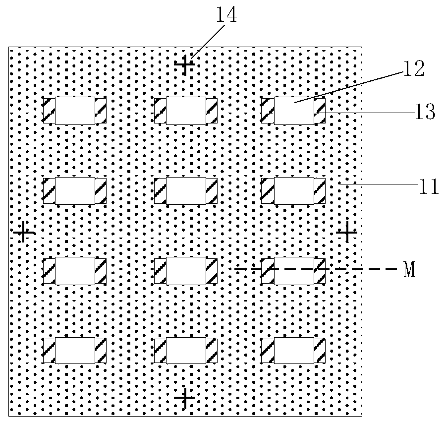
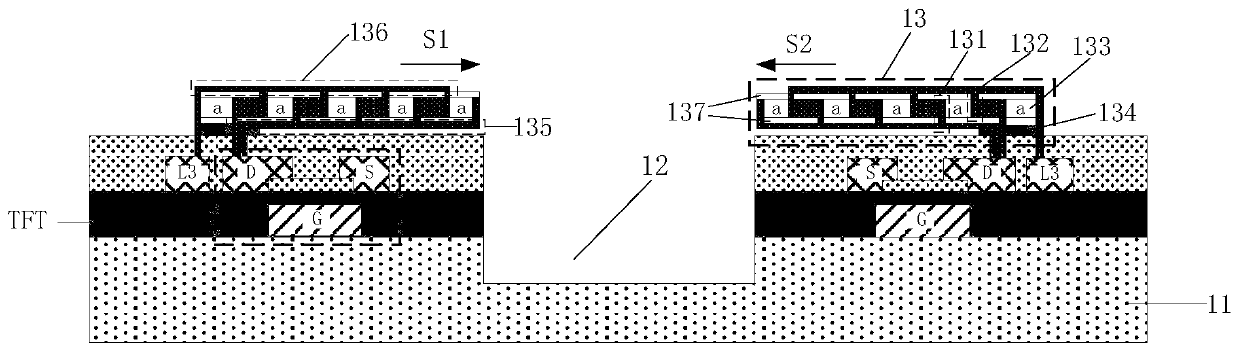
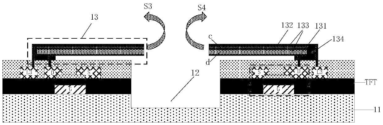
[0061] In the first aspect, the embodiment of the present invention provides a mass transfer head, such as figure 1 As shown, it includes: a transfer substrate 11, a plurality of accommodating grooves 12 for accommodating ligh...


PUM


Abstract

The invention discloses a huge transfer printing head, a transfer printing device and a transfer method of a light emitting diode chip; the huge transfer printing head comprises a transfer printing substrate, a plurality of containing grooves which are positioned in the transfer printing substrate and are used for containing the light-emitting diode chips, electrostriction devices which are positioned on the transfer printing substrate and are located on the edges of the containing grooves, and a first electrode and a second electrode which are positioned between the transfer printing substrate and the electrostriction devices, wherein the first electrode and the second electrode are connected with the electrostriction devices, and are used for applying a first signal or a second signal tothe electrostriction devices; the electrostriction devices are used for moving towards the containing grooves under the control of the first electric signal, so as to shield the part of the openingsof the containing grooves, and moving away from the containing grooves under the control of the second electric signal so as to expose the openings of the containing grooves. According to the huge transfer printing head provided by the embodiment of the invention, a plurality of containing grooves and corresponding electroluminescent devices are arranged on the transfer printing substrate, so thatsimultaneous transfer of the plurality of light-emitting diode chips can be realized.

Description

technical field [0001] The invention relates to the field of display technology, in particular to a mass transfer printing head, transfer printing equipment and a method for transferring light-emitting diode chips. Background technique [0002] With the development of light emitting diode (Light Emitting Diode, LED), Micro-LED display technology will become the next generation of revolutionary technology, because Micro-LED display technology also has liquid crystal display (Liquid Crystal Display, LCD ) and organic light-emitting diode display (Organic Light-Emitting Diode, OLED), and it overcomes the problem of short lifespan of OLED display blue light, Micro-LED display technology can be applied to small augmented reality display (Augmented Reality, AR) or virtual Reality (Virtual Reality, VR) display is as large as billboard movie screen display, and Micro-LED display technology is also suitable for flexible wearable devices. One of the key technologies currently limitin...

Claims


Application Information

Patent Timeline
Patent Type & Authority Applications(China)
IPC IPC(8): H01L21/683H01L21/687H01L27/15
Inventor 刘英伟梁爽狄沐昕梁志伟王珂任庆荣
Owner BOE TECH GRP CO LTD
Why Eureka
Try Eureka