Display panel and manufacturing method thereof and motherboard

A technology for display panels and motherboards, applied in semiconductor/solid-state device manufacturing, electrical components, electric solid-state devices, etc., can solve problems such as high cost and complicated process

Active Publication Date: 2019-09-20
BOE TECH GRP CO LTD +1
View PDF6 Cites 21 Cited by
  • Summary
  • Abstract
  • Description
  • Claims
  • Application Information

AI Technical Summary

Problems solved by technology

[0005] Embodiments of the present invention provide a display panel, a manufacturing method thereof, and a mot...

Method used


Image

  • Display panel and manufacturing method thereof and motherboard
  • Display panel and manufacturing method thereof and motherboard
  • Display panel and manufacturing method thereof and motherboard

Examples


Embodiment Construction

[0057] In view of the complicated process and high cost of the mass transfer technology in the prior art, embodiments of the present invention provide a display panel, a manufacturing method thereof, and a motherboard.

[0058] The specific implementations of the display panel, the manufacturing method thereof, and the motherboard provided by the embodiments of the present invention will be described in detail below with reference to the accompanying drawings. The thickness and shape of each film layer in the drawings do not reflect the true ratio, and the purpose is only to illustrate the content of the present invention schematically.

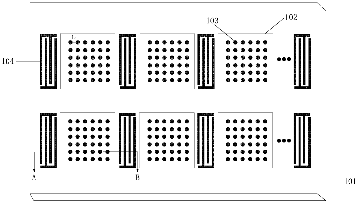
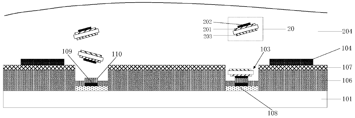
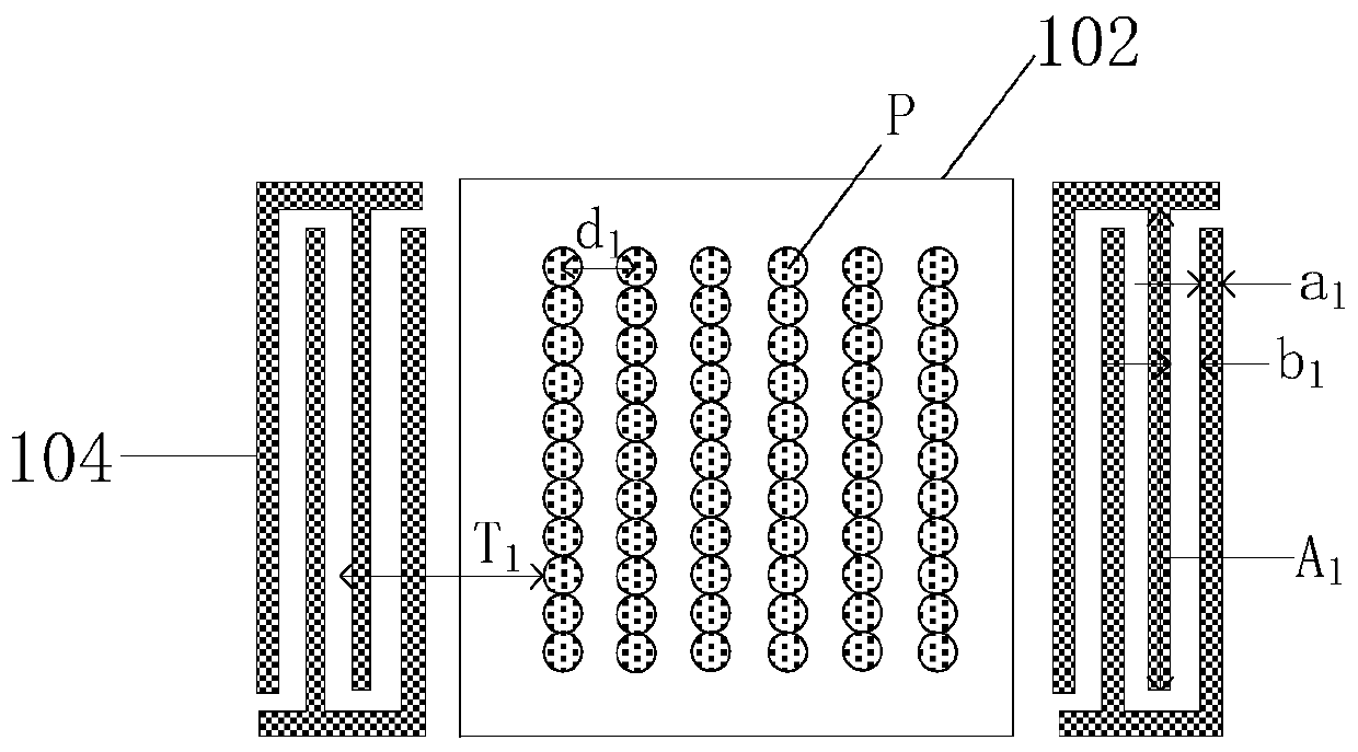
[0059] In the first aspect, an embodiment of the present invention provides a motherboard, such as figure 1 with figure 2 Shown, where, figure 1 Is a schematic structural diagram of a motherboard provided by an embodiment of the present invention, figure 2 for figure 1 The cross-sectional schematic diagram at the midline section AB includes: a ba...


PUM


Abstract

The invention discloses a display panel and a manufacturing method thereof and a motherboard. The motherboard comprises an underlying substrate, a plurality of target regions located on the underlying substrate, and a piezoelectric thin film and an acoustic excitation structure which are located on the underlying substrate. The acoustic excitation structure is located in the region apart from all the target regions and is in contact with the piezoelectric thin film. The acoustic excitation structure is used for generating a surface acoustic wave under the control of a driving signal. Each target region comprises an insulating layer located on the substrate and a plurality of grooves which are used for accommodating micro light-emitting diodes and located on the side of the insulating layer away from the substrate. The piezoelectric thin film is located in the region apart from all the grooves. Each groove is internally provided with a driving electrode and a first magnetic structure. The motherboard can realize massive transfer of the micro light-emitting diodes, the manufacturing process is simple and efficient and the process cost can be effectively reduced.

Description

Technical field [0001] The present invention relates to the field of display technology, in particular to a display panel, a manufacturing method thereof, and a motherboard. Background technique [0002] Micro-LED has the advantages of fast response time, high image quality, high contrast, high color gamut, long life, and low power consumption. Micro-LED has developed into one of the hot spots of display technology in the future. However, currently Micro LED technology faces many technical challenges. Among them, the mass transfer technology in the Micro LED process is currently the most difficult key process. [0003] Specifically, the technical difficulties in the Micro LED process are: After the Micro LED photolithography step, the LED bare chip particles need to be directly transferred from the sapphire substrate to the target substrate, and the lead electrode on the LED needs to be connected to the target substrate. And each transfer volume is very large, and the stability an...

Claims


Application Information

Patent Timeline
IPC IPC(8): H01L27/15H01L21/67H01L21/68H01L33/00
CPCH01L27/156H01L21/67144H01L33/0095H01L21/68
Inventor 付帮然李兴亮高英强陈华斌宋勇志
Owner BOE TECH GRP CO LTD
Why Eureka
Try Eureka