A plasma processing device and method for balancing etching rate

An etching rate and plasma technology, which is applied in semiconductor/solid-state device manufacturing, discharge tubes, electrical components, etc., can solve the problems of reduced surface height of the focus ring, uneven etching rate, and influence of wafer etching process, etc.

Active Publication Date: 2021-06-08
ADVANCED MICRO FAB EQUIP INC CHINA
View PDF4 Cites 0 Cited by
  • Summary
  • Abstract
  • Description
  • Claims
  • Application Information

AI Technical Summary

Problems solved by technology

The surface height of the focus ring decreases, the plasma sheath above it moves down, and the etching process in the edge area of ​​the wafer changes, resulting in uneven etching rates in the center area and edge area of ​​the wafer, which affects the etching process of the wafer

Method used


Image

  • A plasma processing device and method for balancing etching rate
  • A plasma processing device and method for balancing etching rate
  • A plasma processing device and method for balancing etching rate

Examples


Embodiment Construction

[0024] based on the following Figure 2 to Figure 5 , specifically explain the preferred embodiment of the present invention.

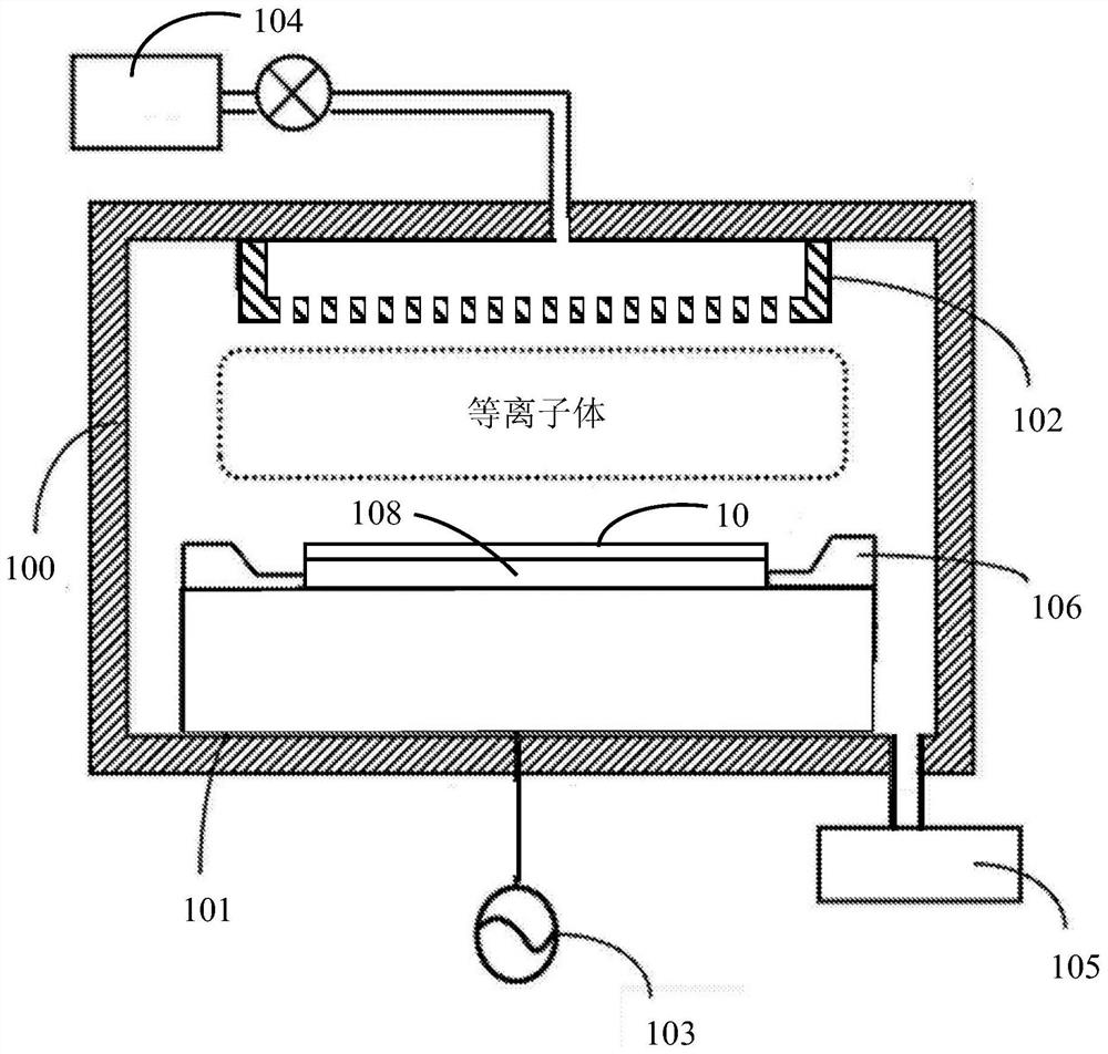
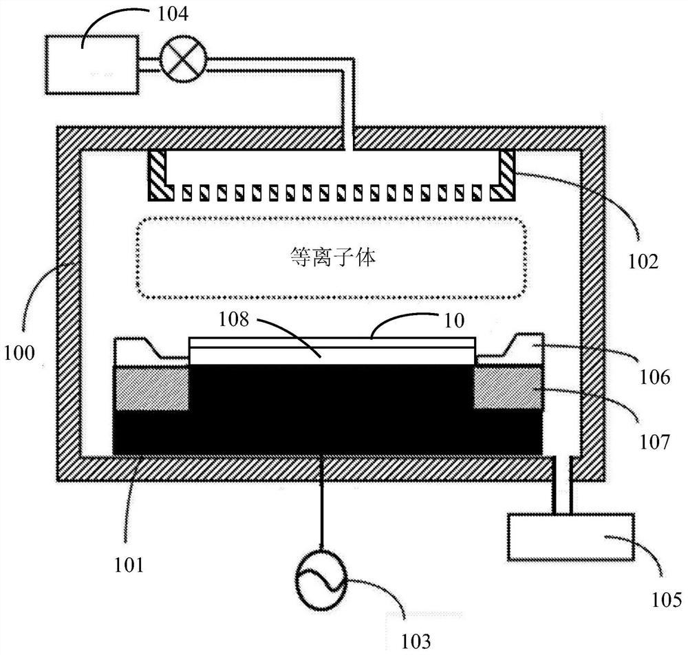
[0025] like figure 2 As shown, the plasma processing device includes a reaction chamber 100, and the reaction chamber 100 is provided with an upper electrode 102 and a lower electrode 101 arranged parallel to each other, and the upper electrode 102 is connected to a reaction gas source 104, and the gas in the reaction gas source 104 passes through the upper electrode 102 is uniformly injected into the interior of the reaction chamber 100. A radio frequency power source 103 is applied on the lower electrode 101, and the radio frequency power source 103 forms a high radio frequency energy field between the upper electrode 102 and the lower electrode 101, and dissociates the reaction gas injected into the reaction chamber 100 into the plasma required for the process , etch the wafer 10 . The lower electrode 101 is also used as a base for supporting t...


PUM


Abstract

A plasma processing device and method for balancing the etching rate. An upper electrode and a lower electrode are arranged in a reaction chamber, a radio frequency power source is applied to the lower electrode, an electrostatic chuck is arranged on the lower electrode, and the electrostatic chuck supports and holds a wafer. The ring is arranged around the wafer, and a capacitance adjustment device is arranged around the lower electrode to change the total capacitance value between the lower electrode and the upper surface of the focus ring, and adjust the lower electrode through the capacitance adjustment device according to the bias power applied to the focus ring. The total capacitance between the electrodes and the upper surface of the focus ring maintains a constant etch rate at the edge and center of the wafer. The invention can effectively adjust the plasma distribution on the surface of the wafer to obtain a uniform and stable etching rate, ensure the uniformity of etching in the edge area and the central area of ​​the wafer, greatly prolong the service life of the focus ring, and save costs.

Description

technical field [0001] The invention relates to the field of semiconductor manufacturing, in particular to a plasma processing device and method for balancing etching rates. Background technique [0002] like figure 1 As shown, the plasma processing device includes a reaction chamber 100, and the reaction chamber 100 is provided with an upper electrode 102 and a lower electrode 101 arranged parallel to each other, and the upper electrode 102 is connected to a reaction gas source 104, and the gas in the reaction gas source 104 passes through the upper electrode 102 is uniformly injected into the interior of the reaction chamber 100. A radio frequency power source 103 is applied on the lower electrode 101, and the radio frequency power source 103 forms a high radio frequency energy field between the upper electrode 102 and the lower electrode 101, and dissociates the reaction gas injected into the reaction chamber 100 into the plasma required for the process , etch the wafer...

Claims


Application Information

Patent Timeline
Patent Type & Authority Patents(China)
IPC IPC(8): H01J37/32H01L21/67
Inventor 赵馗丁冬平
Owner ADVANCED MICRO FAB EQUIP INC CHINA
Why Eureka
Try Eureka