A method for preparing a transparent conductive nanowire grid film on a three-dimensional microstructure surface

A transparent conductive, conductive nanotechnology, applied in the field of photoelectric detection, can solve the problems of reduced light transmittance, increased resistance, difficulty in taking into account light transmittance and reliable electrical path, etc., and achieve good results

Active Publication Date: 2020-07-03
XIAN TECH UNIV
View PDF7 Cites 0 Cited by
  • Summary
  • Abstract
  • Description
  • Claims
  • Application Information

AI Technical Summary

Problems solved by technology

However, if the thickness of the metal film is too small, it will be difficult to form a reliable continuous electrical path, and the resistance will increase sharply. If the thickness is large, the light transmittance will be significantly reduced, and it is difficult to balance good light transmittance and reliable electrical path.

Method used


Image

  • A method for preparing a transparent conductive nanowire grid film on a three-dimensional microstructure surface
  • A method for preparing a transparent conductive nanowire grid film on a three-dimensional microstructure surface
  • A method for preparing a transparent conductive nanowire grid film on a three-dimensional microstructure surface

Examples


Embodiment example

[0027] A high-efficiency visible light detection structure and manufacturing method of the present invention will be further described below in conjunction with the accompanying drawings and specific implementation examples.

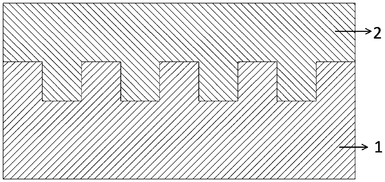
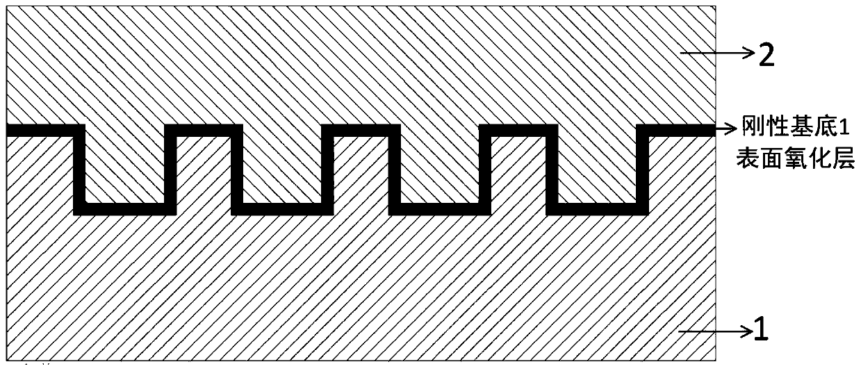
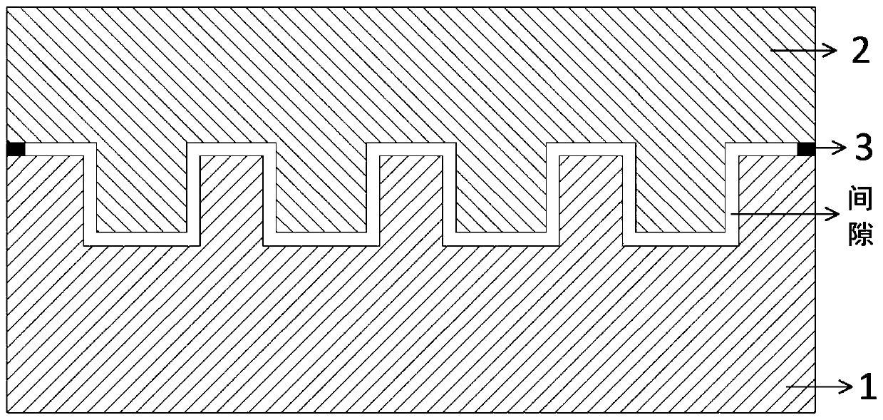
[0028] The present invention is a method for preparing a transparent conductive nanowire grid film on the surface of a three-dimensional microstructure, specifically as follows: the material of the rigid substrate 1 is a material that can be oxidized at high temperature and the oxide layer can be removed by etching. In this embodiment, it is preferably monocrystalline silicon. The material of the flexible press plate 2 is a material that can be embossed, and in this embodiment it is preferably PDMS.

[0029] Such as figure 1 As shown, first a three-dimensional microstructure is fabricated on the upper surface of a single crystal silicon wafer, and the single crystal silicon wafer with a three-dimensional microstructure on the surface is a rigid substrate...


PUM


Abstract

The invention discloses a method for preparing a transparent conductive nanowire mesh film on the surface of a three-dimensional microstructure. The method comprises the steps of making a rigid substrate with a three-dimensional microstructure on the upper surface, making a matched flexible pressing plate with the rigid substrate as a template by using an imprint method, coating the three-dimensional microstructure of the rigid substrate with a conductive nanowire mixed solution and pressing down with the flexible pressing plate to maintain a certain gap between the flexible pressing plate andthe rigid substrate, and drying the conductive nanowire mixed solution in the gap to obtain the nanowire mesh film attached to the surface of the three-dimensional microstructure of the rigid substrate. Conductive nanowires overlapping each other in a mesh achieve the circuit conduction, transparent mesh openings between the nanowires achieve transparency, and the preparation of the transparent conductive nanowire mesh film on the surface of the three-dimensional microstructure is achieved. Micro steps are formed by using a method of etching after oxidation before coating the rigid substratewith the conductive nanowire mixed solution, and the size of the gap can be controlled by the cooperation of the micro steps and the flexible pressing plate. The transparent conductive nanowire mesh film has the advantages of high quality, high preparation efficiency and low cost.

Description

technical field [0001] The invention belongs to the technical field of photoelectric detection, and in particular relates to a method for preparing a transparent conductive nanowire grid film on the surface of a three-dimensional microstructure. Background technique [0002] The function of the photodetector is to convert optical signals into electrical signals. The basic principle is that sensitive materials generate photo-generated carriers under the action of light waves, and the generated photo-generated carriers are collected by electrodes and flow out to the external circuit to form photocurrent. Photodetectors are used in a wide variety of applications, such as imaging, detection, industrial automation, and photometry. In photodetectors, electrodes are essential components. Electrodes in most photodetectors widely used at present are fabricated on planar structures, which is a mature technology. However, with the development of photodetector devices, it has become a...

Claims


Application Information

Patent Timeline
Patent Type & Authority Patents(China)
IPC IPC(8): H01L31/18H01L31/0224B82Y40/00
CPCY02P70/50
Inventor 刘欢刘卫国白民宇王卓曼韩军舒利利敬娟刘蓉
Owner XIAN TECH UNIV
Why Eureka
Try Eureka