Physical vapor deposition process for semiconductor interconnection structures

A conductive filling and substrate technology, applied in semiconductor devices, semiconductor/solid-state device manufacturing, semiconductor/solid-state device components, etc., can solve problems such as no occurrence, improper control, and deterioration of electrical properties of device structures

Active Publication Date: 2019-07-09
TAIWAN SEMICON MFG CO LTD
View PDF7 Cites 4 Cited by
  • Summary
  • Abstract
  • Description
  • Claims
  • Application Information

AI Technical Summary

Problems solved by technology

However, scaling down also creates challenges that may not have been present with the larger geometries of the previous generation
Inaccurate and improper control of deposition and patterning processes during metallized interconnect fabrication can severely deteriorate the electrical performance of device structures

Method used


Image

  • Physical vapor deposition process for semiconductor interconnection structures
  • Physical vapor deposition process for semiconductor interconnection structures
  • Physical vapor deposition process for semiconductor interconnection structures

Examples


Embodiment Construction

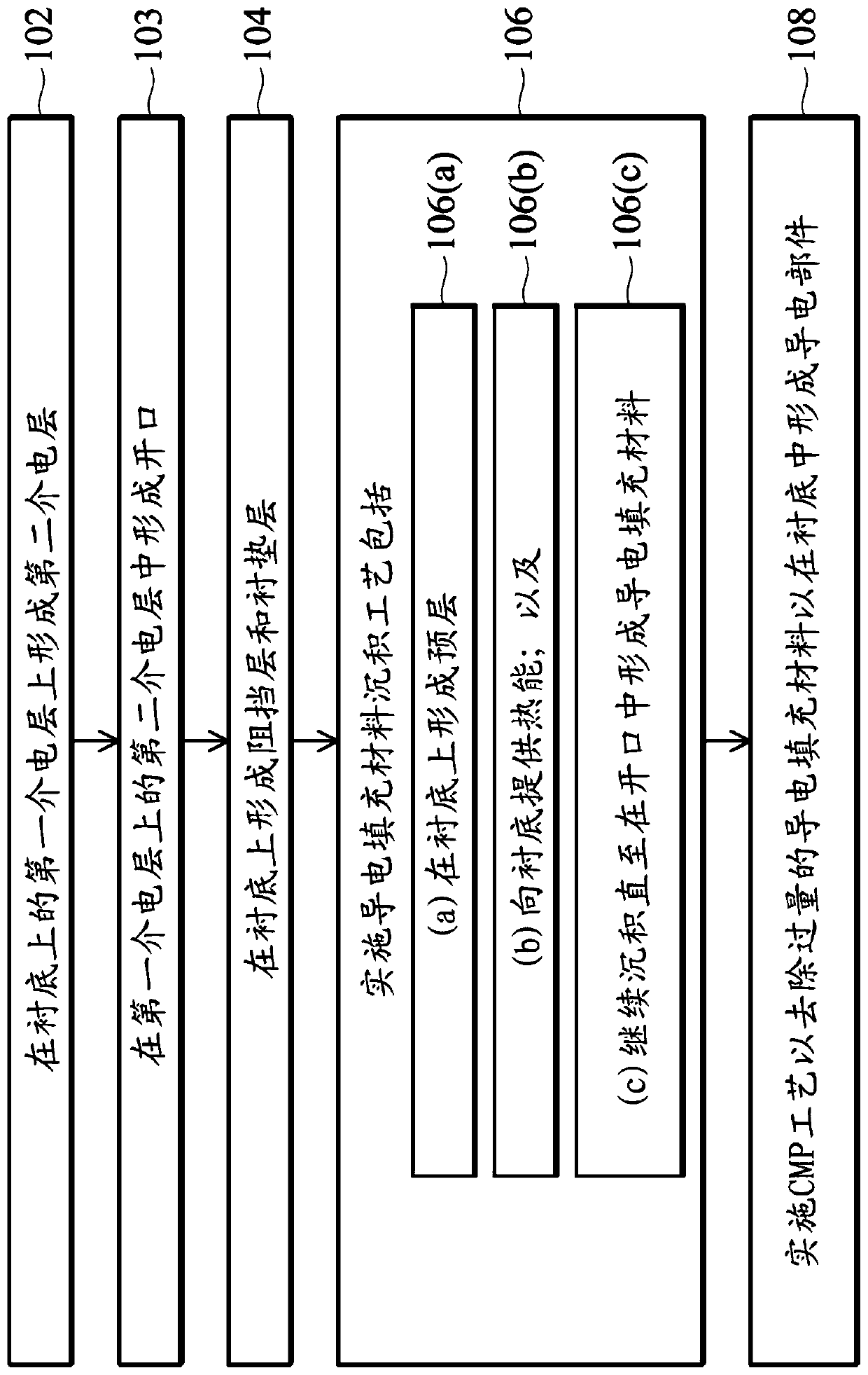
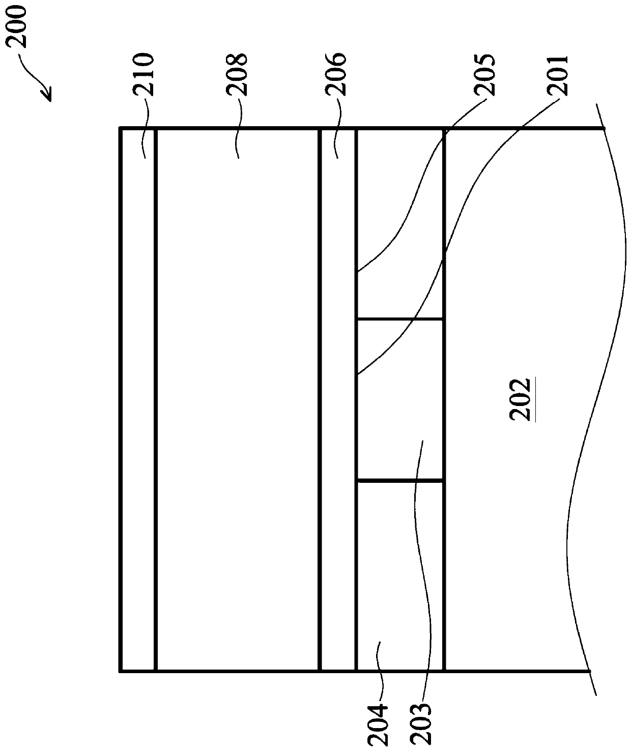
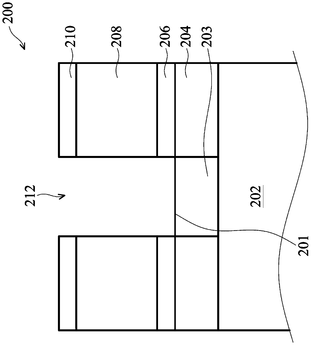
[0012] The following disclosure provides many different embodiments or examples for implementing different features of the presented subject matter. Specific examples of components and arrangements are described below to simplify the present disclosure. Of course, these are examples only and are not intended to limit the invention. For example, in the following description, forming a first component on or on a second component may include an embodiment in which the first component and the second component are formed in direct contact, and may also include an embodiment in which an additional component may be formed between the first component and the second component. components so that the first component and the second component may not be in direct contact with each other. In addition, the present invention may repeat reference numerals and / or characters in various embodiments. This repetition is for the sake of simplicity and clarity and does not in itself indicate a rel...


PUM


Abstract

The present invention provides methods for forming a conductive fill material (e.g., a conductive feature) by a physical vapor deposition (PVD) process. In one embodiment, a method of forming a conductive fill material on a substrate includes maintaining a first substrate temperature at a first range for a first period of time while forming a pre-layer of a conductive fill material on a substrate,providing a thermal energy to the substrate to maintain the substrate at a second substrate temperature at a second range for a second period of time, with the second substrate temperature being higher than the first substrate temperature; and continuously providing the thermal energy to the substrate to maintain the substrate a third substrate temperature at a third range for a third period of time to form a bulk layer of the conductive fill material on the substrate. Embodiments of the invention relate to a physical vapor deposition process used for a semiconductor interconnection structure.

Description

technical field [0001] Embodiments of the present invention relate to physical vapor deposition processes for semiconductor interconnect structures. Background technique [0002] The semiconductor integrated circuit (IC) industry has experienced exponential growth. Technological advances in IC materials and design have produced generations of ICs, where each generation has smaller and more complex circuits than the previous generation. In the course of IC evolution, functional density (eg, the number of interconnected devices per chip area) has generally increased, while geometry size (eg, the smallest component (or line) that can be created using a fabrication process) has decreased. This scaling down process generally provides benefits by increasing production efficiency and reducing associated costs. However, scaling down also creates challenges that may not have been present with the larger geometries of the previous generation. Inaccurate and inadequate control of th...

Claims


Application Information

Patent Timeline
IPC IPC(8): H01L21/768H01L23/535
CPCH01L21/76832H01L21/76829H01L23/535H01L23/53238H01L21/76877H01L21/76864H01L21/02631H01L21/2855H01L21/67103H01L21/324
Inventor 杨乃豪苏鸿文陈冠嘉
Owner TAIWAN SEMICON MFG CO LTD
Why Eureka
Try Eureka