
Preparation method of micro-led display panel and micro-led display panel

A technology for display panels and LED arrays, applied in semiconductor devices, electrical components, circuits, etc., can solve the problem of high difficulty in bonding of micro LEDs, and achieve the effects of avoiding alignment and bonding, avoiding abnormal display, and reducing the difficulty of alignment

Active Publication Date: 2020-12-25
CHENGDU VISTAR OPTEOLECTRONICS CO LTD
View PDF7 Cites 0 Cited by
  • Summary
  • Abstract
  • Description
  • Claims
  • Application Information

AI Technical Summary

Problems solved by technology

[0004] In view of this, the object of the present invention is to propose a method for preparing a micro-LED display panel and a micro-LED display panel to solve the problem of high bonding difficulty of micro-LEDs during mass transfer, and to improve the yield and efficiency of mass transfer

Method used

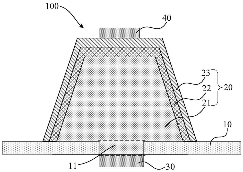
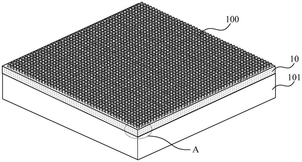

Image

  • Preparation method of micro-led display panel and micro-led display panel
  • Preparation method of micro-led display panel and micro-led display panel
  • Preparation method of micro-led display panel and micro-led display panel

Examples


Embodiment Construction

[0060] The technical solutions of the present invention will be further described below in conjunction with the accompanying drawings and through specific implementation methods. It should be understood that the specific embodiments described here are only used to explain the present invention, but not to limit the present invention. In addition, it should be noted that, for the convenience of description, only some structures related to the present invention are shown in the drawings but not all structures.

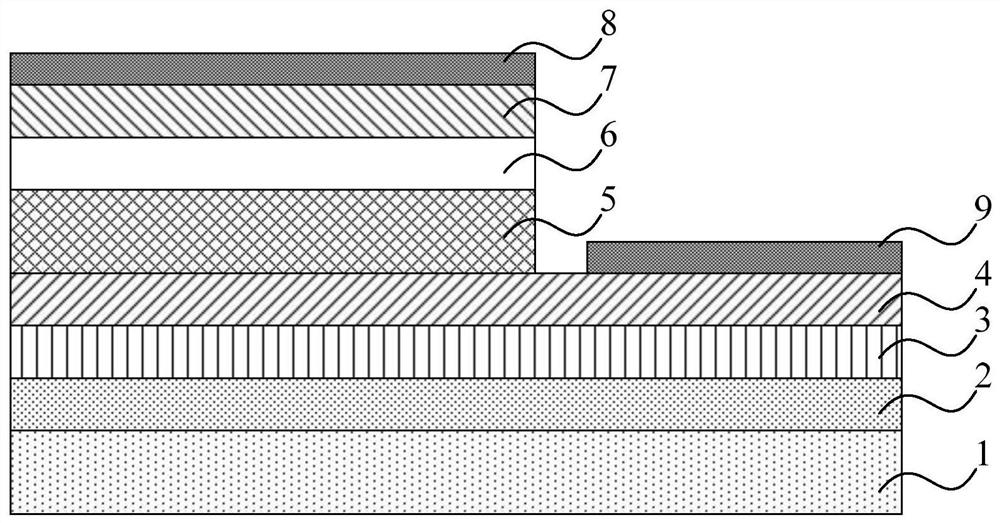
[0061] figure 1 is a schematic diagram of a micro-LED structure in the prior art, such as figure 1 As shown, the micro LED structure includes a substrate 1, a nucleation layer 2, a non-doped GaN layer 3, an n-type GaN layer 4, a multi-quantum well layer 5, an electron blocking layer 6 and a p-type GaN layer 7 stacked in sequence, Among them, part of the multi-quantum well layer 5, the electron blocking layer 6 and the p-type GaN layer 7 are etched away, a p-electrode 8...


PUM

PropertyMeasurementUnit
thicknessaaaaaaaaaa
pore sizeaaaaaaaaaa

Abstract

The invention discloses a preparation method of a micro LED display panel and the micro LED display panel. The method comprises steps that a mask layer is formed on a first substrate, and openings arearranged in an array on the mask layer; an LED epitaxial structure grows at each opening; one side of the mask layer adjacent to the LED epitaxial structure is formed with a second electrode electrically connected with a second type semiconductor layer in each of the LED epitaxial structures; the LED epitaxial structures are transferred to a second substrate; the first substrate is stripped off;one side of the mask layer away from the LED epitaxial structures is formed with a first electrode electrically connected with a first type semiconductor layer in each of the LED epitaxial structures;the LED epitaxial structures are bonded to a target substrate through the first electrode; the second substrate is stripped off. The method is advantaged in that a problem of high binding difficultyduring huge-amount transfer of micro LEDs is solved, and the huge-amount transfer yield and efficiency are improved.

Description

technical field [0001] The embodiments of the present invention relate to the field of micro-LED display technology, and in particular to a method for preparing a micro-LED display panel and the micro-LED display panel. Background technique [0002] Light Emitting Diodes (LEDs) are widely used in technical fields such as lighting and display due to their advantages of small size, low power, long service life, high brightness and active light emission. Micro LED, also known as micro LED, mLED or μLED, is a new type of flat panel display technology. The micro LED display has an LED array of individual pixel elements. Compared with the widely used liquid crystal display, the micro LED display has a better contrast ratio. , Faster response speed, lower energy consumption. [0003] Since micro-LEDs are manufactured individually in the form of chips, the size of which is on the order of microns, therefore, in the process of manufacturing display devices, it is necessary to transf...

Claims


Application Information

Patent Timeline
Patent Type & Authority Patents(China)
IPC IPC(8): H01L33/00H01L27/15
CPCH01L27/156H01L33/0095H01L33/0093
Inventor 樊腾邢汝博韦冬郭恩卿孙建明
Owner CHENGDU VISTAR OPTEOLECTRONICS CO LTD
Learn More