
Image acquisition device for flat scanner

A technology of image acquisition device and scanner, which is applied in the direction of image communication, electrical components, etc. It can solve the problems of insufficient attention to the optimization of the acquisition end and affect the scanning quality, etc., and achieve the effect of fast signal conversion output and not easy to cause excessive signal noise

Active Publication Date: 2019-07-09
东莞蓝海宽场光电科技有限公司
View PDF5 Cites 0 Cited by
  • Summary
  • Abstract
  • Description
  • Claims
  • Application Information

AI Technical Summary

Problems solved by technology

[0004] In the image acquisition and processing of the scanner, the image acquisition is designed and analyzed through experiments. During the scanning process, the LED illumination color, intensity and subsequent signal conversion of the CIS have a greater impact on the optical scanning quality, so the acquisition part of the scanning system is also becomes particularly critical, but the market does not pay enough attention to the optimization of the acquisition end, which affects the overall scanning quality

Method used


Image

  • Image acquisition device for flat scanner
  • Image acquisition device for flat scanner
  • Image acquisition device for flat scanner

Examples


Embodiment Construction

[0021] In order to facilitate the understanding of those skilled in the art, the present invention will be further described below in conjunction with the examples, and the contents mentioned in the embodiments are not intended to limit the present invention.

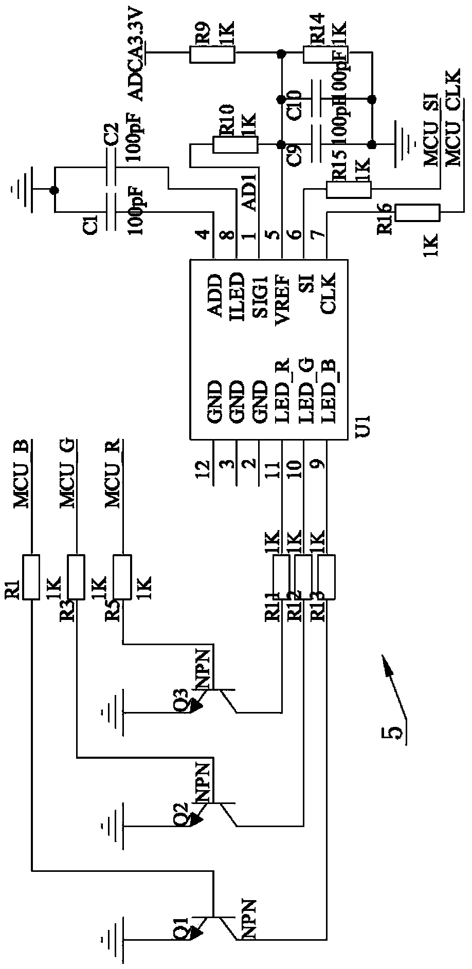
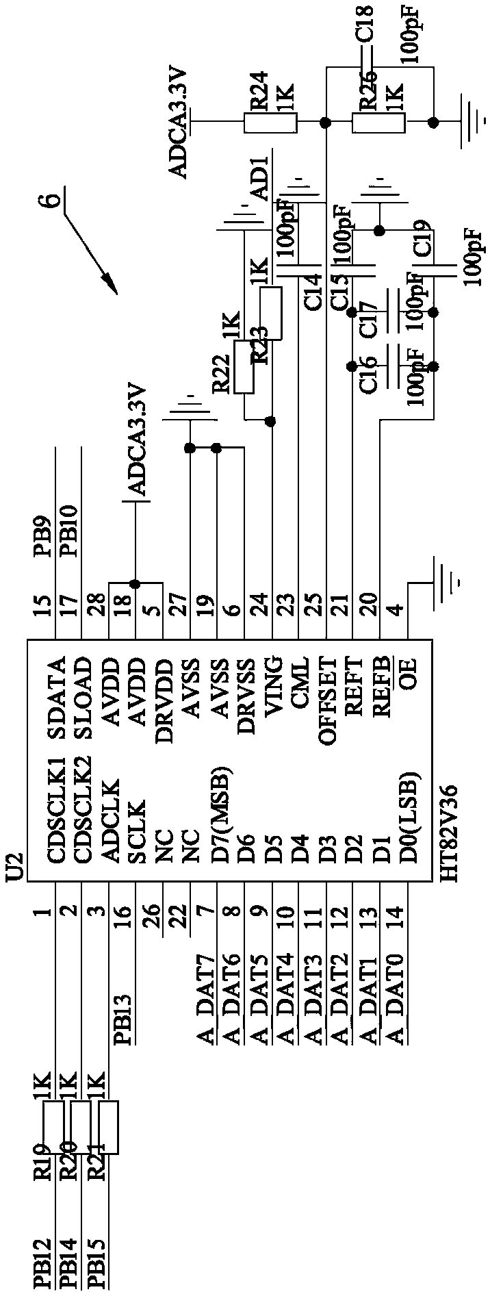
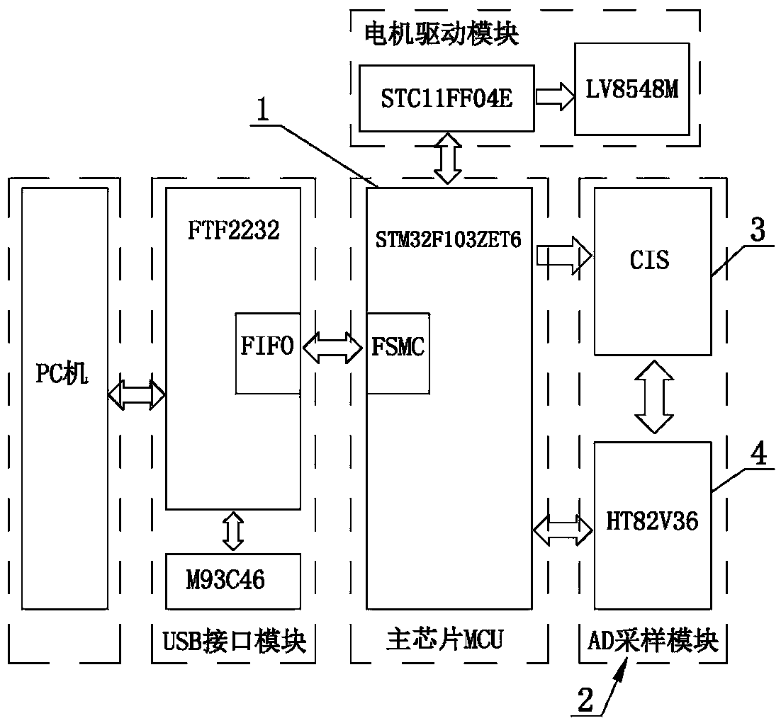
[0022] Such as Figure 1 to Figure 3 As shown, an image acquisition device for a flatbed scanner includes an MCU main chip 1 and an AD sampling module 2 that is electrically connected to the MCU main chip 1. The CIS acquisition unit 3 and the HT82V36 analog-to-digital conversion unit 4, wherein the CIS acquisition unit circuit 5 is provided with a processor U1, and the eleventh end of the processor U1 is connected in series with a resistor R11, a transistor Q3 and a resistor R5 in series, and the first end of the processor U1 Resistor R12, transistor Q2 and resistor R3 are connected in series at terminal 10, resistor R13, transistor Q1 and resistor R1 are connected in series at terminal 9 of processor U1, and the other ...


PUM


Abstract

The invention relates to the technical field of scanning equipment, in particular to an image acquisition device for a flat scanner. An AD sampling module comprises a CIS acquisition unit and an HT82V36 analog-to-digital conversion unit which are in electric signal connection with an MCU main chip, wherein the 11th end of the CIS acquisition unit processor U1 is sequentially connected with a resistor R11, a triode Q3 and a resistor R5 in series; the tenth end of the processor U1 is sequentially connected with a resistor R12, a triode Q2 and a resistor R3 in series; the ninth end of the processor U1 is sequentially connected with a resistor R13, a triode Q1 and a resistor R1 in series; the other end of the resistor R5, the other end of the resistor R3 and the other end of the resistor R1 are all connected with the MCU main chip. By optimizing the control circuit of the CIS, the light emitting intensity and the lighting-on and lighting-off speeds of the LED lamp in the CIS are better controlled, signal conversion and output are better and more quickly completed, and the situations that signal noise is too high and damage occurs are not likely to happen.

Description

technical field [0001] The invention relates to the technical field of scanning equipment, in particular to an image acquisition device for a flatbed scanner. Background technique [0002] Flatbed scanners are widely used in many fields and are important opto-mechanical-electrical integration equipment. The work of the flatbed scanner is mainly to convert the optical signal of the image into an analog signal, and then convert it into a digital signal that the computer can recognize. After the appearance of CCD image sensor and CMOS image sensor, the scanning image acquisition equipment can be electronicized and digitized. With the development of electronic computer technology, digital image acquisition and processing technology has developed rapidly, and the resolution, acquisition speed, integration degree, and reliability have all been greatly improved. [0003] According to the image sensor, scanners can be divided into CIS scanners and CCD scanners. CIS is a new type ...

Claims


Application Information

Patent Timeline
Patent Type & Authority Applications(China)
IPC IPC(8): H04N1/10H04N1/031
CPCH04N1/031H04N1/10
Inventor 李清顺陈子豪叶腾铭董日浴
Owner 东莞蓝海宽场光电科技有限公司
Learn More