
Radio frequency chip fan-out system-level packaging process

A technology of system-level packaging and radio frequency chips, applied in the direction of electrical components, semiconductor/solid-state device manufacturing, circuits, etc., can solve problems such as secondary damage to chips, and achieve the effect of avoiding damage

Active Publication Date: 2019-07-12
浙江集迈科微电子有限公司
View PDF3 Cites 1 Cited by
  • Summary
  • Abstract
  • Description
  • Claims
  • Application Information

AI Technical Summary

Problems solved by technology

[0005] Traditional fan-out packaging often requires rewiring and TSV interconnection after the chip is attached to the adapter board, which is likely to cause secondary damage to the chip

Method used


Image

  • Radio frequency chip fan-out system-level packaging process
  • Radio frequency chip fan-out system-level packaging process
  • Radio frequency chip fan-out system-level packaging process

Examples


Embodiment Construction

[0034] Embodiments of the present invention are described in detail below, wherein the same or similar reference numerals represent the same or similar elements or elements with similar functions. The embodiments described below by referring to the figures are exemplary, and are only used to explain the present invention and not to limit the present invention.

[0035] Those skilled in the art can understand that, unless otherwise defined, all terms (including technical terms and scientific terms) used herein have the same meanings as commonly understood by those of ordinary skill in the art to which this invention belongs. It should also be understood that terms such as those defined in commonly used dictionaries should be understood to have a meaning consistent with the meaning in the context of the prior art, and unless defined as herein, will not be used in an idealized or overly formal meaning to explain.

[0036] The reference numerals related to the steps mentioned in ...


PUM

PropertyMeasurementUnit
Thicknessaaaaaaaaaa
Thicknessaaaaaaaaaa
Thicknessaaaaaaaaaa

Abstract

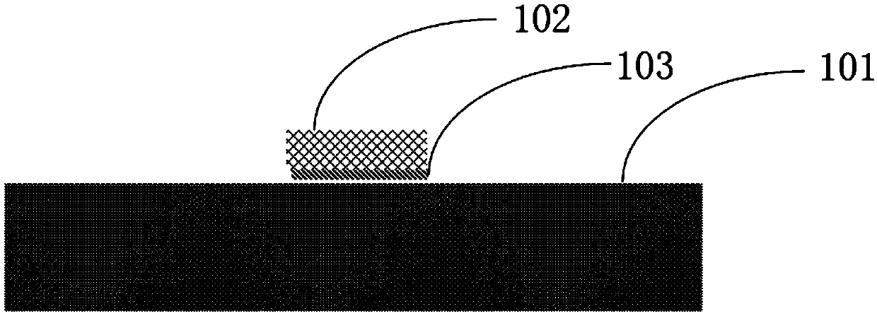
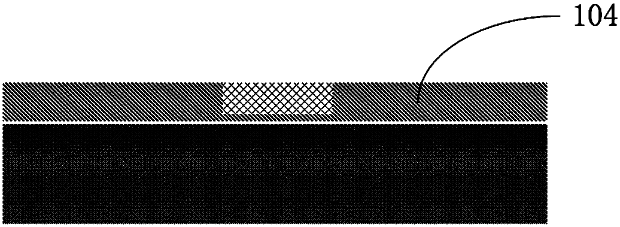
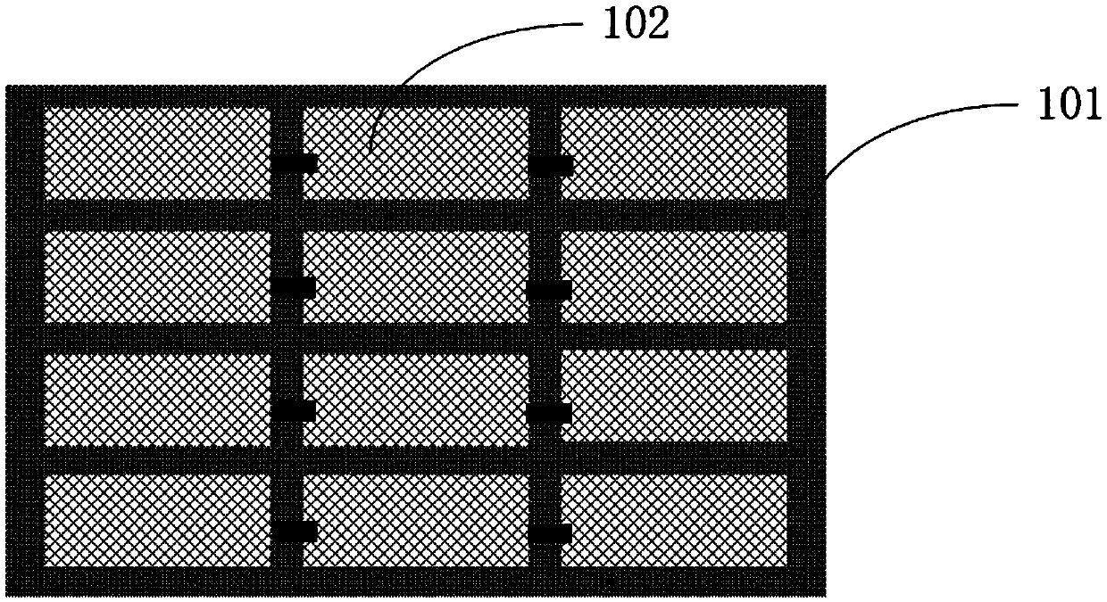
The invention discloses a radio frequency chip fan-out system-level packaging process comprising the following steps of (101) carrier processing, (102) base processing, and (103) packaging. The present invention provides the radio frequency chip fan-out system-level packaging process, and the damage to a chip by secondary processing is avoided.

Description

technical field [0001] The invention relates to the technical field of semiconductors, more specifically, it relates to a radio frequency chip fan-out type system-in-package process. Background technique [0002] Millimeter wave radio frequency technology is developing rapidly in the semiconductor industry. It is widely used in high-speed data communication, automotive radar, airborne missile tracking system, and space spectrum detection and imaging. It is expected that the market will reach 1.1 billion US dollars in 2018 and become an emerging industry. New applications put forward new requirements for the electrical performance, compact structure and system reliability of the product. For the wireless transmitting and receiving system, it cannot be integrated into the same chip (SOC) at present, so it is necessary to integrate different chips including the radio frequency unit , filters, power amplifiers, etc. are integrated into an independent system to realize the functi...

Claims


Application Information

Patent Timeline
IPC IPC(8): H01L21/768
CPCH01L21/76895H01L21/76898
Inventor 冯光建丁祥祥陈雪平马飞程明芳郭丽丽郑赞赞郁发新
Owner 浙江集迈科微电子有限公司
Learn More