
Silicon controlled rectifier

一种硅控整流器、重掺杂区的技术,应用在整流器领域,能够解决低电流释放能力等问题

Active Publication Date: 2019-07-16
AMAZING MICROELECTRONICS
View PDF3 Cites 0 Cited by
  • Summary
  • Abstract
  • Description
  • Claims
  • Application Information

AI Technical Summary

Problems solved by technology

However, the traditional zener diode triggered silicon controlled rectifier occupies a large area of ​​silicon, and also faces the problem of low current release capability per unit area

Method used

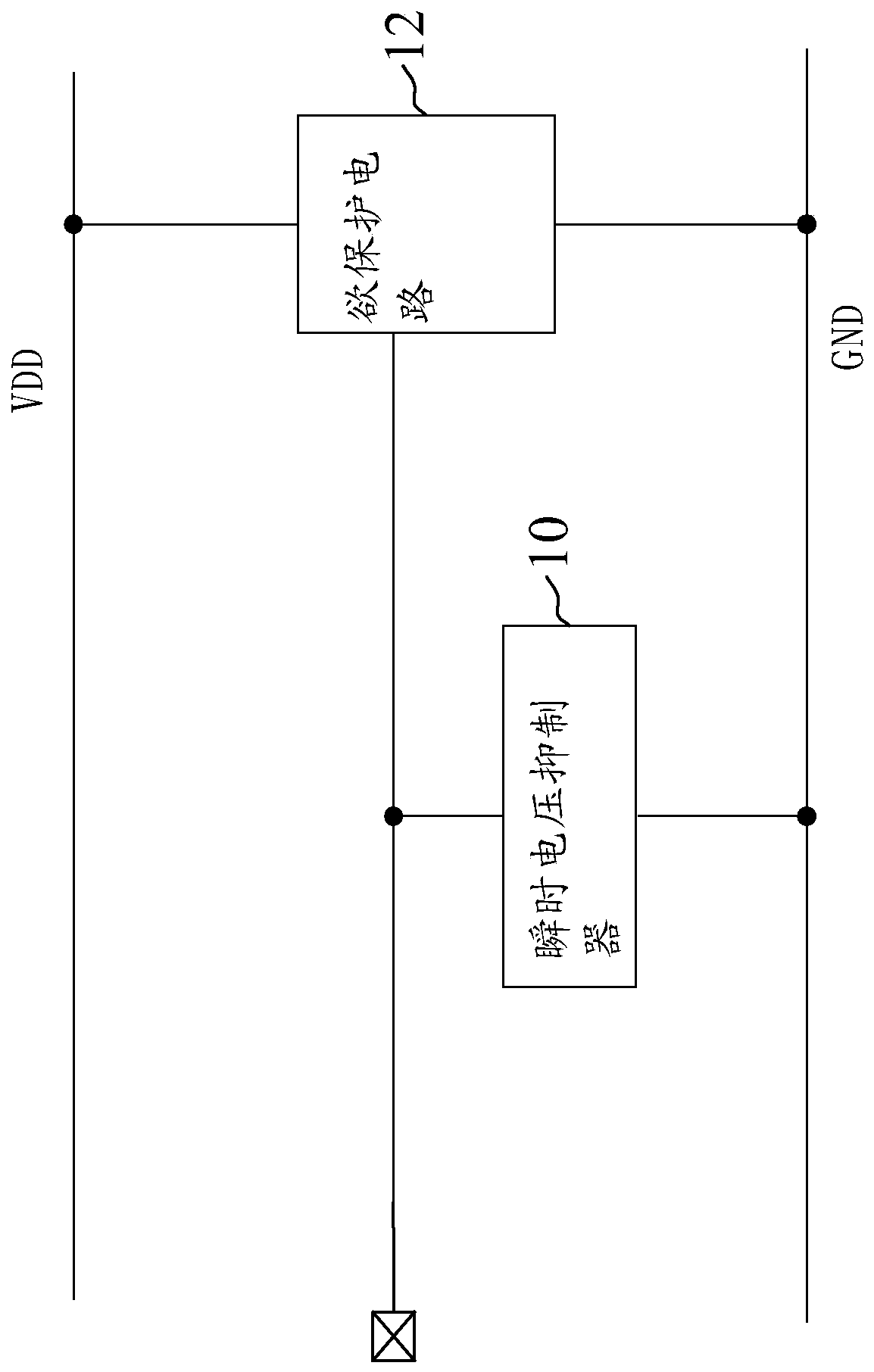

Image

  • Silicon controlled rectifier
  • Silicon controlled rectifier
  • Silicon controlled rectifier

Examples


no. 1 example

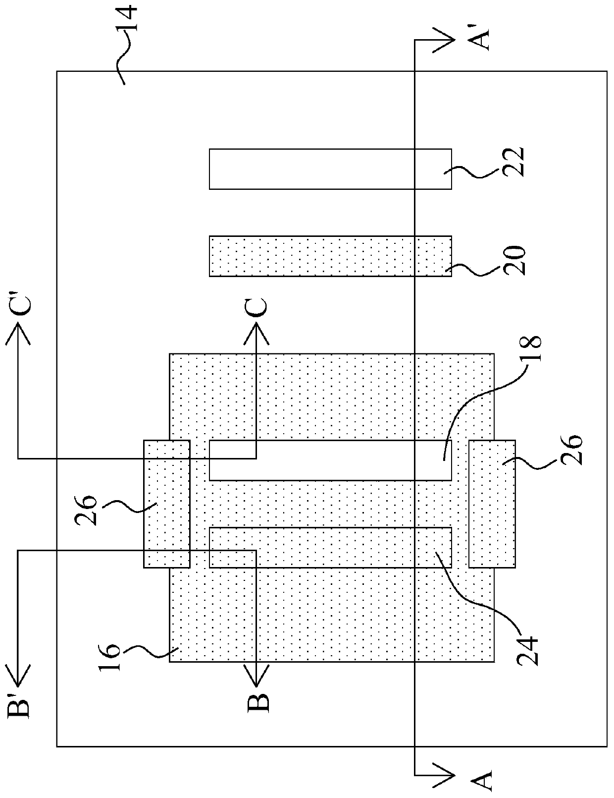
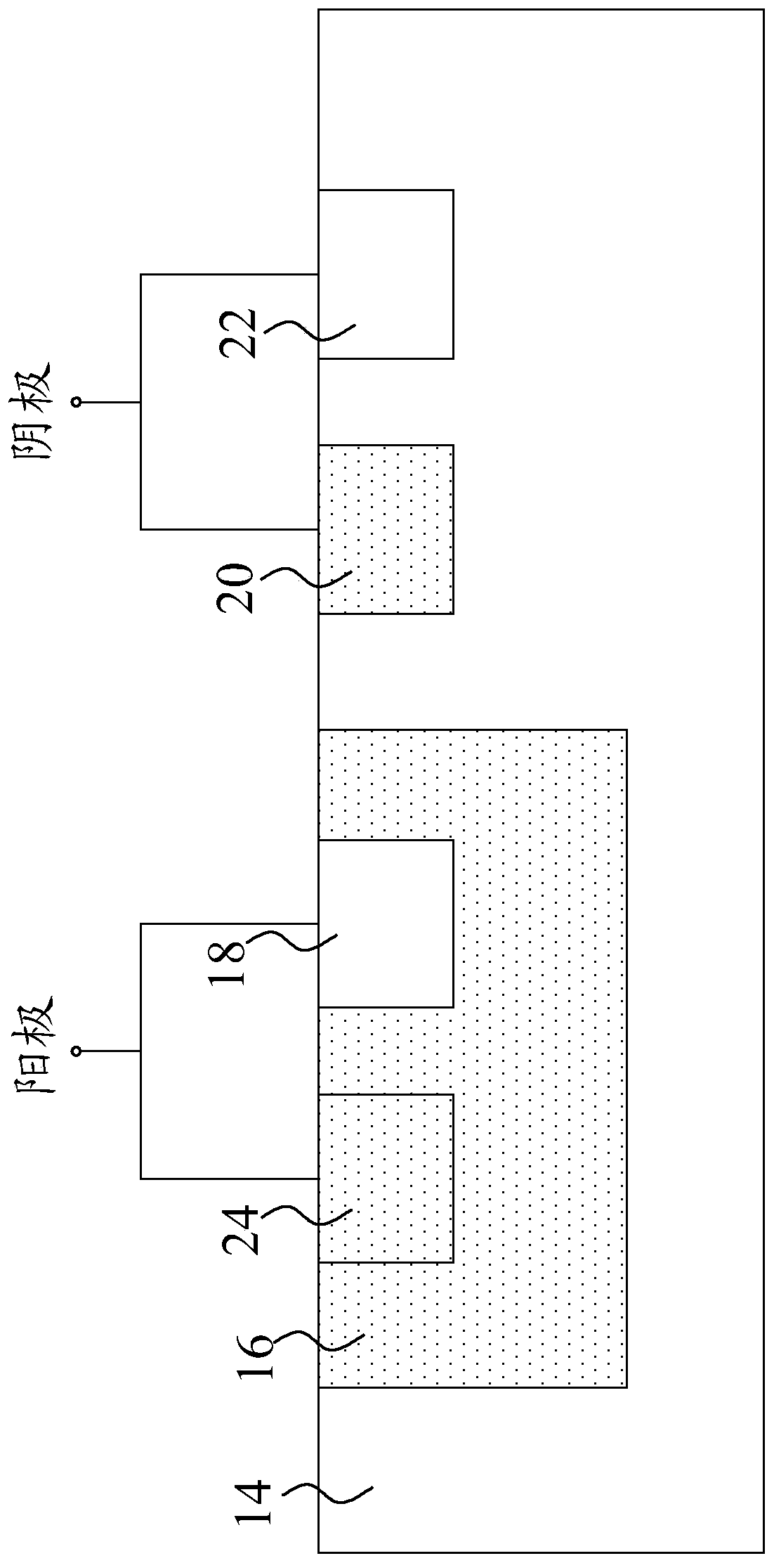
[0049] See below figure 2 , image 3 , Figure 4 and Figure 5 . The following introduces the first embodiment of the silicon controlled rectifier of the present invention, which includes a P-type substrate 14, an N-type doped well region 16, a first P-type strip heavily doped region 18, a first N-type strip Shaped heavily doped region 20, a second P-type heavily doped region 22, a second N-type heavily doped region 24, and at least one N-type heavily doped region 26. The N-type doped well region 16 is arranged in the P-type substrate 14, the first P-type strip-shaped heavily doped region 18 is arranged in the N-type doped well region 16, the first N-type strip-shaped heavily doped region 20 and the second The P-type strip-shaped heavily doped region 22 is disposed on the P-type substrate 14 , the second N-type strip-shaped heavily doped region 24 is disposed on the N-type doped well region 16 , and the N-type heavily doped region 26 is disposed on the P-type substrate 14...

no. 7 example

[0057] See below Figure 15 , Figure 16 , Figure 17 and Figure 18 . The seventh embodiment of the silicon controlled rectifier of the present invention is introduced below, which includes an N-type substrate 30, a P-type doped well region 32, a first N-type strip heavily doped region 34, a first P-type strip Shaped heavily doped region 36 , a second N-type heavily doped region 38 , a second P-type heavily doped region 40 and at least one P-type heavily doped region 42 . The P-type doped well region 32 is arranged in the N-type substrate 30, the first N-type strip-shaped heavily doped region 34 is arranged in the P-type doped well region 32, and the first P-type strip-shaped heavily doped region 36 is arranged in the In the N-type substrate 30, the second N-type strip-shaped heavily doped region 38 is arranged in the N-type substrate 30, and the second P-type strip-shaped heavily doped region 40 is arranged in the P-type doped well region 32, and the P-type heavily doped...


PUM


Abstract

The invention discloses a silicon controlled rectifier comprising a P-type substrate, an N-type doped well region, a first P-type strip-shaped heavily-doped region, a first N-type strip-shaped heavily-doped region and at least one N-type heavily-doped region. The first P-type strip-shaped heavily-doped region is arranged in the N-type doped well region, and the first N-type strip-shaped heavily-doped region is arranged in a P-type substrate. The N-type heavily-doped region is arranged in the N-type doped well region and P-type substrate. The N-type heavily-doped region is not arranged betweenthe first P-type strip-shaped heavily-doped region and the first N-type strip-shaped heavily-doped region, so that the surface area of the semiconductor substrate is reduced. The conductivity type ofthe above components can also be changed.

Description

technical field [0001] The present invention relates to a rectifier, and in particular to a silicon controlled rectifier capable of reducing the surface area of ​​a semiconductor substrate. Background technique [0002] Damaged by the impact of electrostatic discharge (ESD), and some electronic products, such as laptops or mobile phones, are also thinner and shorter than before, and the ability to withstand ESD impacts is even lower. For these electronic products, if no proper ESD protection device is used for protection, the electronic products are easily impacted by ESD, causing system restarts of the electronic products, and even hardware damage and irreversible problems. At present, all electronic products are required to pass the ESD test requirements of the IEC 61000-4-2 standard. For the ESD problem of electronic products, using a transient voltage suppressor (TVS) is a more effective solution, so that the ESD energy can be released quickly through the TVS, so as to ...

Claims


Application Information

Patent Timeline
Patent Type & Authority Applications(China)
IPC IPC(8): H01L27/02H01L29/06
CPCH01L27/0207H01L27/0248H01L29/0684H01L27/0262H01L29/0692H01L29/87H01L27/0251H01L29/41716H01L29/74
Inventor 沈佑书李品辉
Owner AMAZING MICROELECTRONICS
Learn More