Feeding device and method of integrated circuit chip testing and sorting machine

A chip testing and feeding device technology, applied in sorting and other directions, can solve the problems of low production efficiency of semiconductor device testing tapes, small size of semiconductor devices, and high difficulty, and achieves high practicability, simple and convenient operation, and stable and reliable work. Effect

Pending Publication Date: 2019-07-19
FUZHOU PALIDE ELECTRONICS TECH
View PDF7 Cites 6 Cited by
  • Summary
  • Abstract
  • Description
  • Claims
  • Application Information

AI Technical Summary

Problems solved by technology

[0002] Semiconductor devices (i.e. chips) need to undergo a series of testing operations before taping. At present, there is no integrated equipment on the market that can complete testing and taping operations at the same time, resulting in low production efficiency of semiconductor device testing and taping.
In addition, due to the small size and light weight of semiconductor devices, it is difficult to realize automatic material feeding, which is also a major bottleneck restricting the development of semiconductor device testing and tape integration equipment.

Method used


Image

  • Feeding device and method of integrated circuit chip testing and sorting machine
  • Feeding device and method of integrated circuit chip testing and sorting machine
  • Feeding device and method of integrated circuit chip testing and sorting machine

Examples


Embodiment Construction

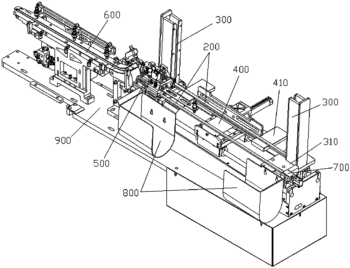
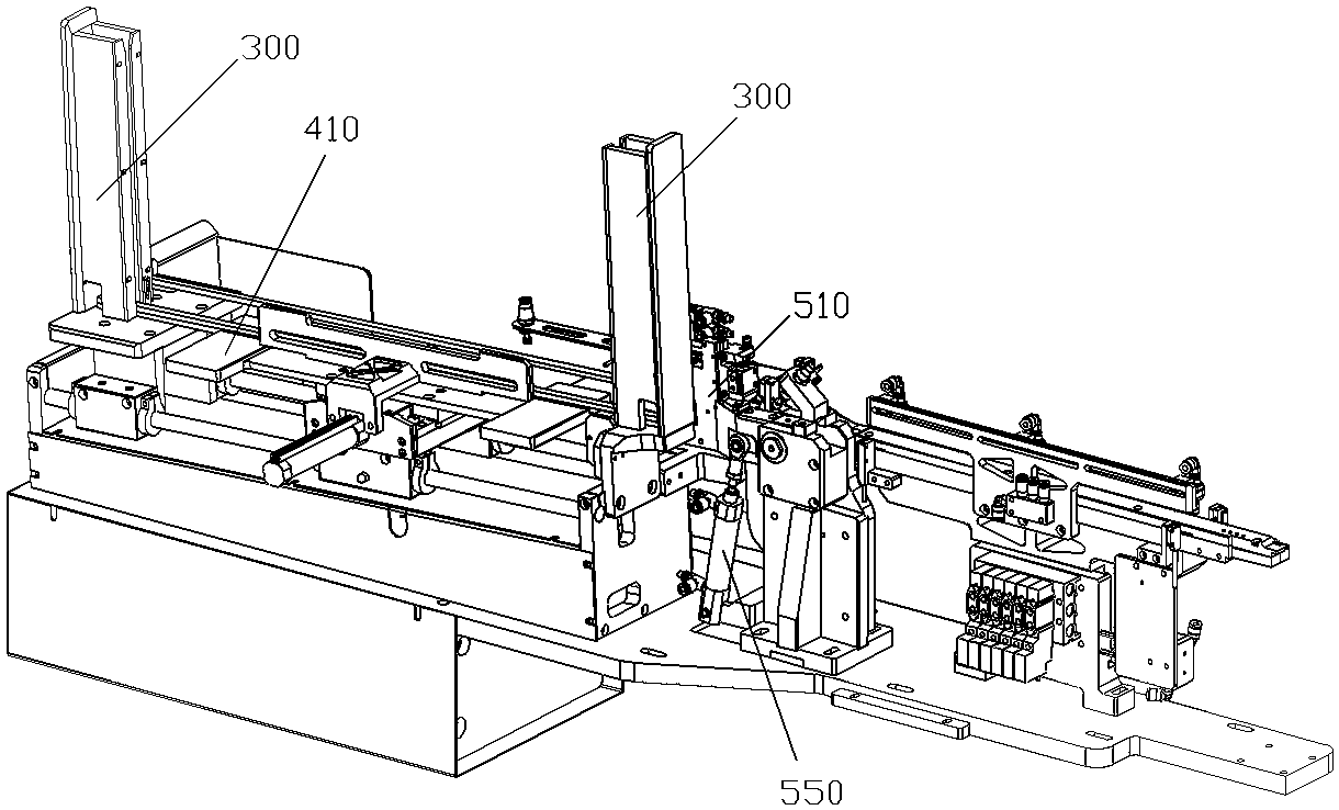
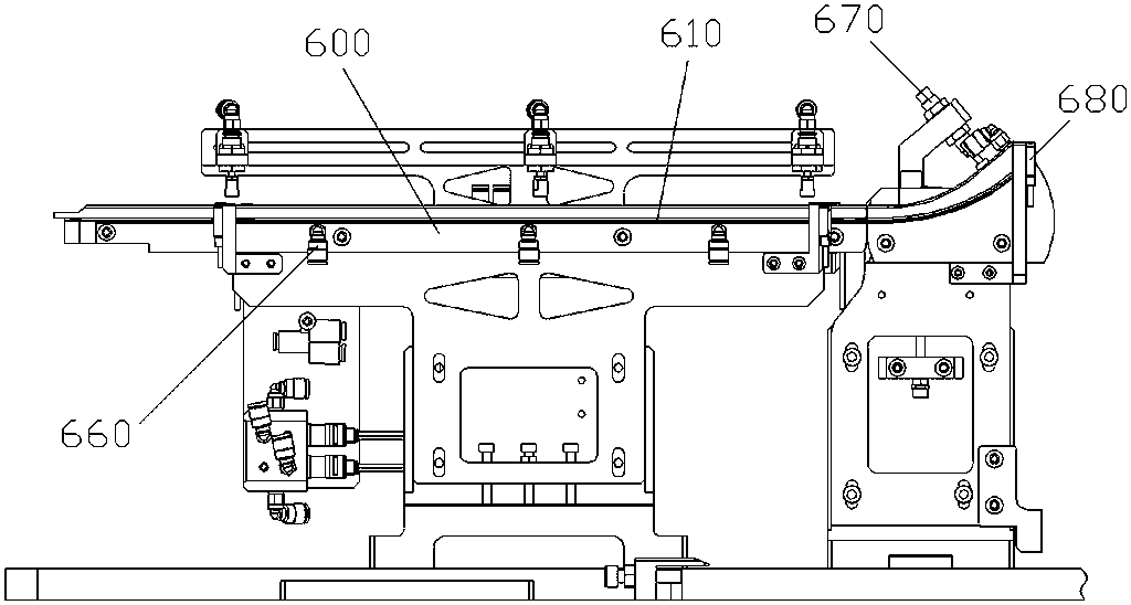
[0026] Such as Figure 1~11 As shown, a feeding device for an integrated circuit chip test sorter includes a frame 900, on which a trough 300 for vertically stacking packaging tubes 200 with semiconductor devices 100 is installed on the frame 900, for The packaging tube for accommodating semiconductor devices is an existing technology, and will not be elaborated again; the internal size of the packaging tube is slightly larger than the size of the semiconductor device, and the semiconductor device can slide freely in the packaging tube. Arranged in a row; two troughs 300 are erected at both ends of the packaging tube, and the two ends of the packaging tube extend into the trough; the side of the bottom of the trough 300 has an outlet for a single packaging tube to pass through 310, a pushing mechanism 400 is provided below the trough 300 to push the lowermost packaging tube from the discharge port; a swing mechanism 500 is provided on the side of the front end of the trough to...


PUM


Abstract

The invention relates to a feeding device and method of an integrated circuit chip testing and sorting machine. The feeding device comprise a rack, wherein a material groove used for vertically stacking packaging pipes provided with semiconductor devices in a single row is arranged on the rack; a discharging port capable of allowing a single packaging pipe to pass is reserved beside the bottom ofthe material groove; a pushing mechanism for pushing the lowest packaging pipe out of the discharging port is arranged below the material groove; a swinging mechanism for swinging the pushed-out packaging pipe to an inclined state is arranged beside the front end of the material groove; a feeding guide rail is arranged in front of the swinging mechanism; a feeding channel used for conveying the semiconductor devices is arranged in the feeding guide rail; and the rear end of the feeding channel is in butt joint with the lower end of the packaging pipe after swinging and inclining. According tothe feeding device of the integrated circuit chip testing and sorting machine, continuous and stable feeding of the semiconductor devices one by one is achieved, the semiconductor devices are not prone to being damaged, the efficiency is high, and the practicability is high; and a worker only needs to stack the packaging pipes with the semiconductor devices in the material groove, and the operation is simple and convenient.

Description

technical field [0001] The invention relates to a feeding device and method for an integrated circuit chip testing and sorting machine. Background technique [0002] Semiconductor devices (i.e. chips) need to undergo a series of testing operations before taping. At present, there is no integrated equipment on the market that can complete testing and taping operations at the same time, resulting in low production efficiency of semiconductor device testing and taping. In addition, due to the small size and light weight of semiconductor devices, it is difficult to realize automatic material feeding, which is also a major bottleneck restricting the development of semiconductor device testing and tape integration equipment. Contents of the invention [0003] In view of this, the object of the present invention is to provide a feeding device and method for an integrated circuit chip testing and sorting machine with convenient operation, stable and reliable operation and high eff...

Claims


Application Information

Patent Timeline
Patent Type & Authority Applications(China)
IPC IPC(8): B07C5/02
CPCB07C5/02
Inventor 谢名富吴成君林康生
Owner FUZHOU PALIDE ELECTRONICS TECH
Why Eureka
Try Eureka