

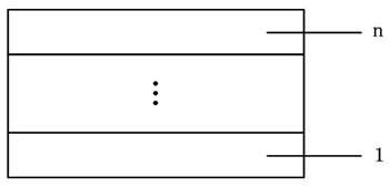
Multilayer transparent electroconductive thin film
A transparent conductive film, amorphous technology, applied in the direction of layered products, etc., can solve the problems of poor electrical conductivity and high resistivity, and achieve the effects of good uniformity, low resistivity, and improved interface contact performance.
- Summary
- Abstract
- Description
- Claims
- Application Information
AI Technical Summary
Problems solved by technology
Method used
Image


Examples
Embodiment 1
[0021] Using glass as a substrate, sequentially depositing InAl on it 0.1 ZnO 3.65 Amorphous oxides, metallic Cu and InAl 0.1 ZnO 3.65 Amorphous oxide, forming 3 layers of amorphous transparent conductive film.
[0022] Prepared by pulsed laser deposition method, the specific steps are as follows:
[0023] 1) with In 2 o 3 、Al 2 o 3 and ZnO powder as the source material, weighed according to the atomic ratio In:Al:Zn=1:0.1:1, and sintered to obtain InAl 0.1 ZnO 3.65 ceramic target.
[0024] 2) Fix the glass substrate on the sample tray after cleaning, put it into the reaction vacuum chamber, and put the InAl 0.1 ZnO 3.65 The ceramic target is mounted on the pulsed laser deposition target head, and the growth chamber is fed with O 2 , control the total pressure to 0.01Pa, raise the substrate temperature to 300°C, deposit 56nm thick amorphous InAl 0.1 ZnO 3.65 film layer.
[0025] 3) Remove the InAl 0.1 ZnO 3.65 For the ceramic target, the pure Cu metal target i...
Embodiment 2
[0029] Using glass as a substrate, metal Cu, InAl are deposited sequentially on it 0.1 ZnO 3.65 Amorphous oxide, forming 2 layers of amorphous transparent conductive film.
[0030] Prepared by pulsed laser deposition method, the specific steps are as follows:
[0031] 1) with In 2 o 3 、Al 2 o 3 and ZnO powder as the source material, weighed according to the atomic ratio In:Al:Zn=1:0.1:1, and sintered to obtain InAl 0.1 ZnO 3.65 ceramic target.
[0032] 2) Fix the glass substrate on the sample tray after cleaning, and put it into the reaction vacuum chamber. Install the pure Cu metal target on the pulsed laser deposition target head, and the vacuum degree of the growth chamber is pumped to 1×10 -3 Pa, a 20 nm thick Cu layer was deposited.
[0033] 3) Remove the pure Cu metal target, InAl 0.1 ZnO 3.65 The ceramic target is installed on the target frame, and then embedded in the target head of the pulsed laser deposition device, and the growth chamber is fed with O ...
Embodiment 3
[0036] Using glass as a substrate, sequentially depositing InSi on it 0.1 ZnO 3.65 Amorphous oxide, metal Ag, InSi 0.1 ZnO 3.65 Amorphous oxide, forming 3 layers of amorphous transparent conductive film.
[0037] Prepared by magnetron sputtering method, the specific steps are as follows:
[0038] 1) with In 2 o 3 , SiO 2 and ZnO powder as the source material, weighed according to the atomic ratio In:Si:Zn=1:0.1:1, and sintered to obtain InSi 0.1 ZnO 3.65 ceramic target.
[0039] 2) Fix the glass substrate on the sample tray after cleaning, put it into the reaction vacuum chamber, and put the InSi 0.1 ZnO 3.65 The ceramic target is installed on the magnetron sputtering target head, and the growth chamber is connected to O 2 , the total pressure is controlled at 1.5Pa, the substrate temperature is raised to 300°C, and 80nm thick amorphous InSi is deposited 0.1 ZnO 3.65 film layer.
[0040] 3) Remove the InSi 0.1 ZnO 3.65 For the ceramic target, the pure Ag metal ...
PUM
| Property | Measurement | Unit |
|---|---|---|
| thickness | aaaaa | aaaaa |
| thickness | aaaaa | aaaaa |
| thickness | aaaaa | aaaaa |
Abstract
Description
Claims
Application Information