Group III Nitride Semiconductor Light-Emitting Device and Method of Producing the Same

a technology of nitride and light-emitting devices, which is applied in the direction of semiconductor/solid-state device manufacturing, semiconductor devices, electrical apparatus, etc., can solve the problems of troublesome wiring including wire bonding, deterioration of productivity at the time of mounting operation, and process devices, etc., to achieve excellent thermal conductivity, enhanced productivity at the time of mounting operation, and excellent radiation properties

Active Publication Date: 2007-12-06
TOYODA GOSEI CO LTD
View PDF2 Cites 13 Cited by
  • Summary
  • Abstract
  • Description
  • Claims
  • Application Information

AI Technical Summary

Benefits of technology

[0018] According to the present invention, on a surface of an uppermost layer which is opposite from a crystal substrate used for forming the stacked structure thereon, there is provided a plate body made of material different from that of the crystal substrate, and the crystal substrate is then removed. Thus, the stacked structure is mechanically supported on the plate body, and the ohmic electrode having one polarity is formed on the surface of the conductive plate body. Therefore, the device can directly be mounted, and only an ohmic electrode having the opposite polarity may be subjected to wire bonding and thus, the productivity at the time of the mounting operation is enhanced.
[0019] According to the invention, the conductive Si monocrystal plate is bonded onto the stacked structure used for the light-emitting device so that the monocrystal plate is disposed in parallel to the specific crystal orientation of the sapphire substrate used for forming the stacked structure, thereby forming the Group III nitride semiconductor light-emitting device. Therefore, even if the great forward current should flow over a long time, no crack which might be caused due to thermal stress is generated in the stacked structure. This is why since the warping direction extends along the crystal orientation when the thermal stress is decreased, if the monocrystal plate is bonded onto the opposite side from a side where it is conceived that the plate is warped, the plate is not warped. Since the thermal conductivity is excellent, radiation properties are also excellent. As a result, even if the device is lit for a long time, thermal damage is less prone to be generated, and when high current flows, output is not lowered by heat.

Problems solved by technology

In the case of the flip chip type, it is troublesome to process the device, and in the case of the two-bonding type, the wiring including wire bonding is troublesome.
Thus, there is a problem that the productivity at the time of mounting operation is deteriorated.

Method used


Image

  • Group III Nitride Semiconductor Light-Emitting Device and Method of Producing the Same
  • Group III Nitride Semiconductor Light-Emitting Device and Method of Producing the Same
  • Group III Nitride Semiconductor Light-Emitting Device and Method of Producing the Same

Examples


examples

[0051] The present invention will be described based on a case in which a conductive Si monocrystal plate is bonded as a plate body onto the uppermost layer of a stacked structure to form a Group III nitride semiconductor light-emitting device.

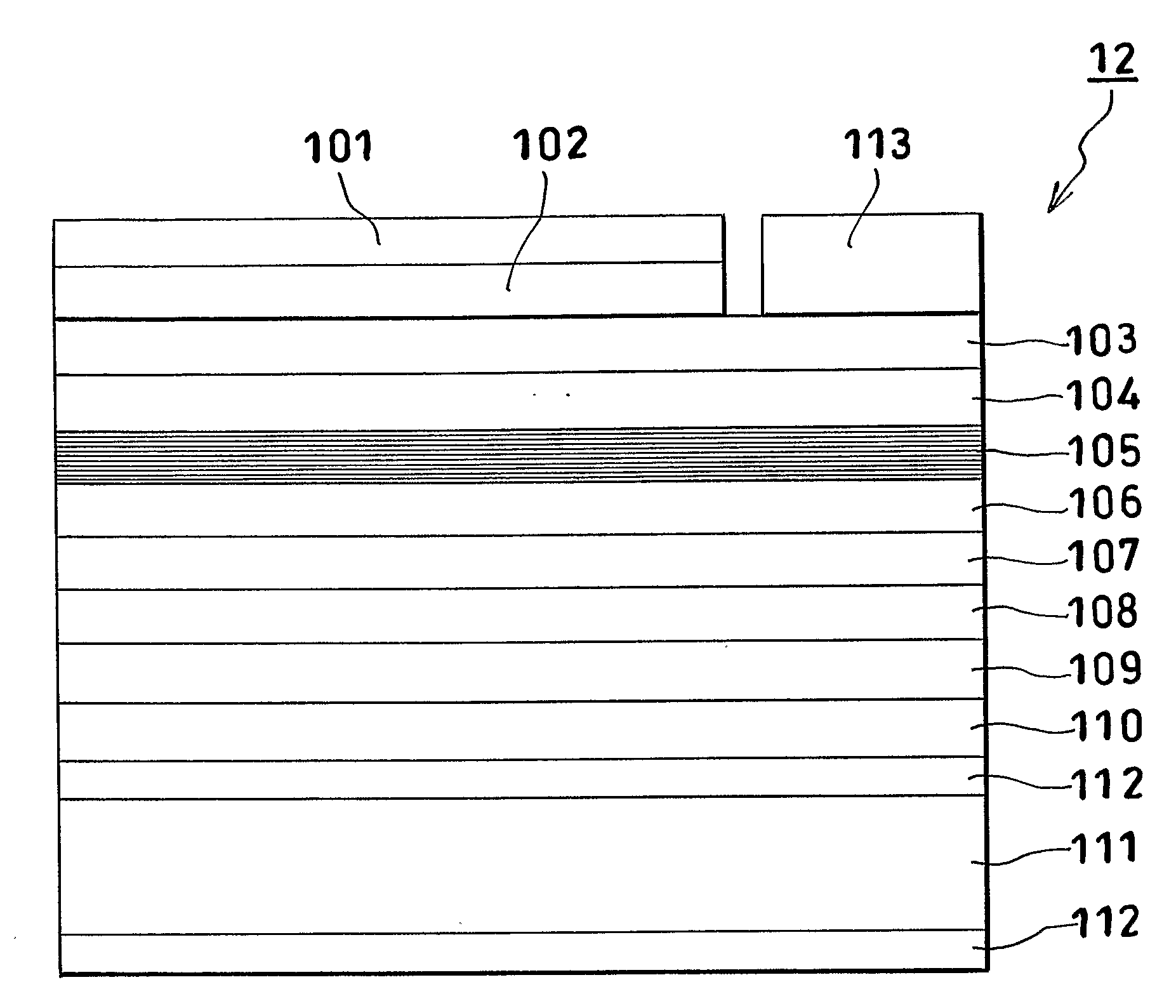
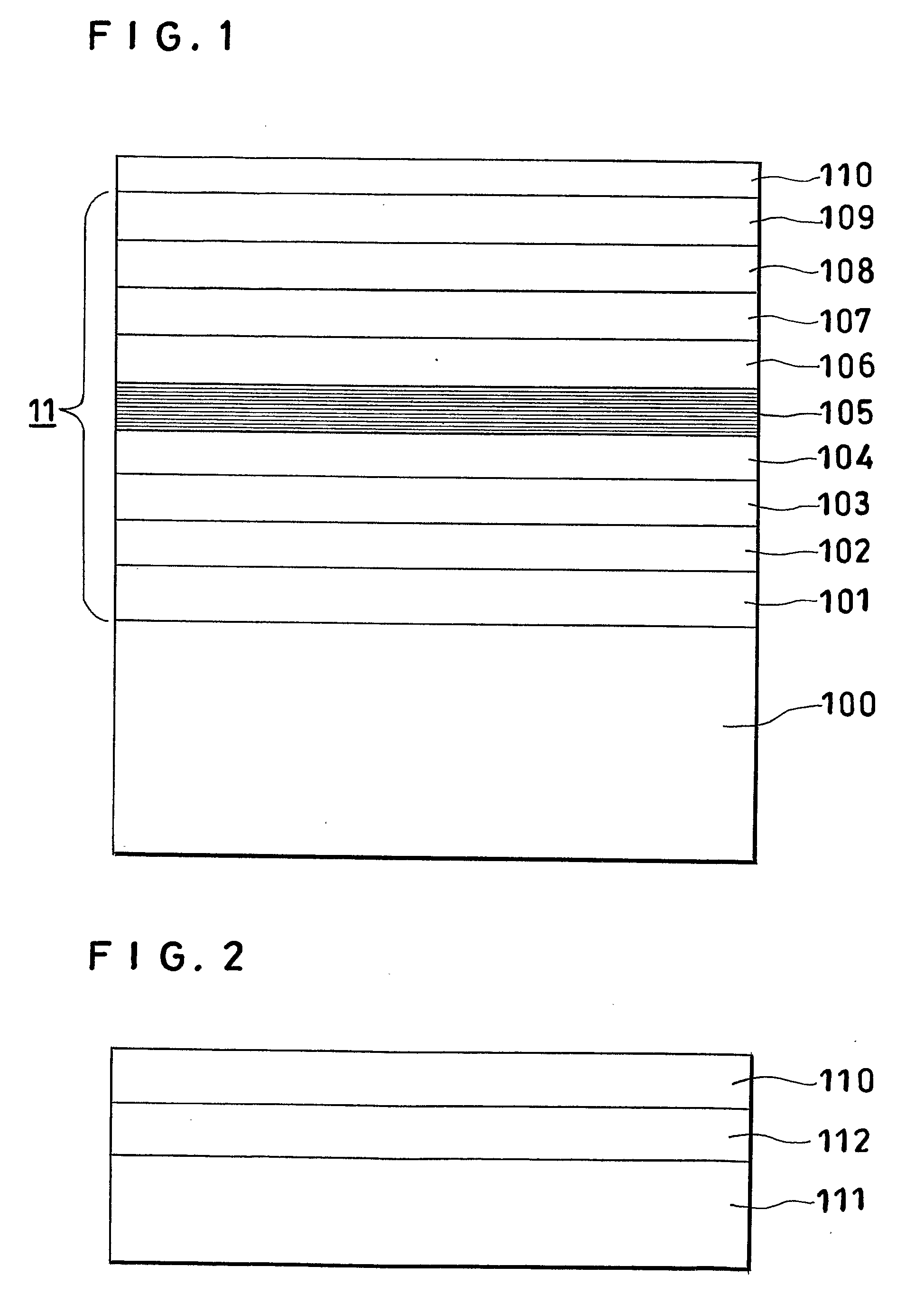
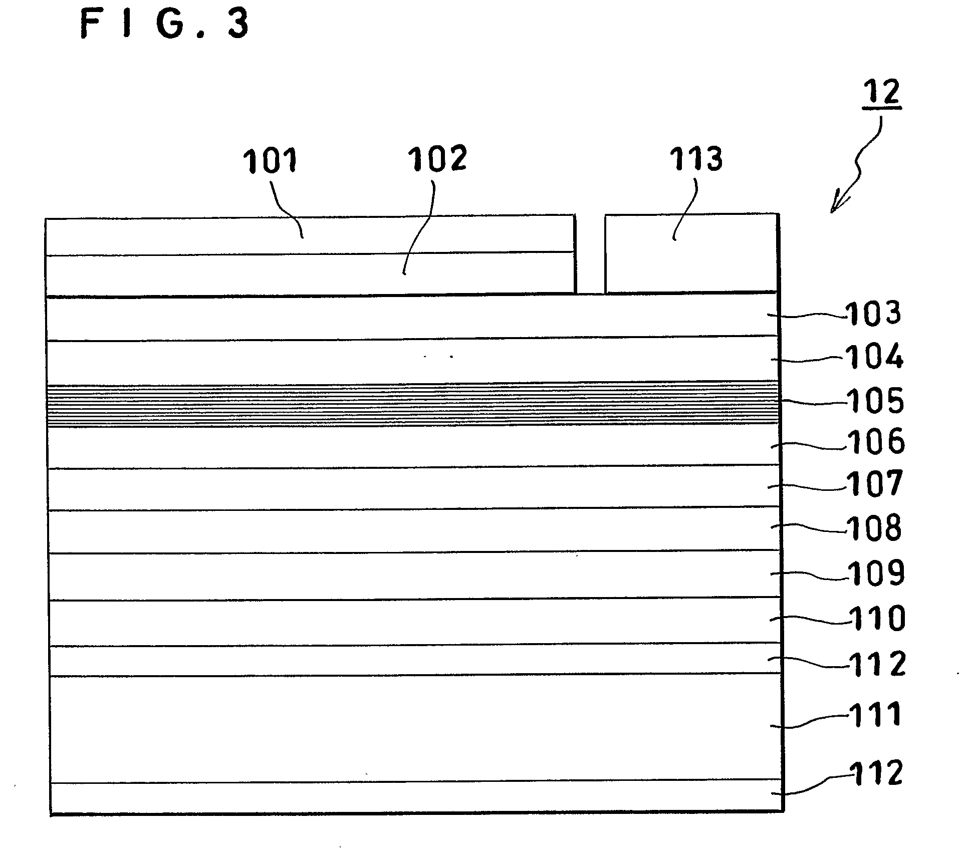
[0052]FIG. 1 is a schematic cross section showing the structure of the stacked structure formed on a sapphire substrate. FIG. 2 shows a structure on the side of the plate body. FIG. 3 is a schematic cross section showing the structure of an LED according to the present invention obtained by chipping the stacked structure shown in FIG. 1. FIG. 4 is a plan view of the LED. FIG. 5 is a sectional view of an LED lamp formed by mounting the LED.

[0053] First, as shown in FIG. 1, an aluminum nitride (AlN) layer 101 was formed on a (0001) crystal face of an electric insulating sapphire substrate 100 about 350 μm in thickness using seeding process (SP) means by means of the ordinary pressure-reduced MOCVD method at 900° C. The thickness of the AlN lay...


PUM

PropertyMeasurementUnit
thicknessaaaaaaaaaa
thicknessaaaaaaaaaa
thicknessaaaaaaaaaa

Abstract

A Group III nitride semiconductor light-emitting device includes a stacked structure 11 formed on a crystal substrate (100) to be removed from it and including two Group III nitride semiconductor layers 104 and 106 having different electric conductive types and a light-emitting layer 105 which is stacked between the two Group III nitride semiconductor layers and which includes a Group III nitride semiconductor, and a plate body 111 made of material different from that of the crystal substrate and formed on a surface of an uppermost layer which is opposite from the crystal substrate that is removed from the stacked structure.

Description

CROSS REFERENCE TO RELATED APPLICATIONS [0001] This application is an application filed under 35 U.S.C. § 111(a) claiming the benefit pursuant to 35 U.S.C. § 119(e) (1) of the filing date of Provisional Application No. 60 / 557,063 filed Mar. 29, 2004 pursuant to 35 U.S.C § 111(b).TECHNICAL FIELD [0002] The present invention relates to a Group III nitride semiconductor light-emitting device comprising a stacked structure including two Group III nitride semiconductor layers having different electric conductive types and a light-emitting layer which is stacked between the two Group III nitride semiconductor layers and which comprises a Group III nitride semiconductor, and to a producing method thereof. BACKGROUND ART [0003] Conventionally, Group III nitride semiconductor light-emitting devices, such as light-emitting diodes (LEDs) which emit short-wavelength light of blue band or green band and laser diodes (LDs), utilize a light-emitting layer of gallium indium nitride (GaYInZN: 0≦Y, Z...

Claims


Application Information

Patent Timeline
Patent Type & Authority Applications(United States)
IPC IPC(8): H01L33/00H01L33/06H01L33/10H01L33/32H01L33/34H01L33/40H01L33/46H01L33/56H01L33/62
CPCH01L33/0079H01L33/32H01L2224/48091H01L2924/00014H01L33/0093
Inventor KUSUNOKI, KATSUKIMITANI, KAZUHIROUDAGAWA, TAKASHI
Owner TOYODA GOSEI CO LTD
Why Eureka
Try Eureka