

Step pulse test method of semiconductor device based on LabVIEW
A pulse test, semiconductor technology, applied in the direction of single semiconductor device testing, instruments, measuring electricity, etc., can solve the problems of inability to meet the needs of efficient and accurate experiments, low ease of use, slow speed, etc., to achieve automatic real-time testing, Simple structure to overcome the effect of low usability
- Summary
- Abstract
- Description
- Claims
- Application Information
AI Technical Summary
Problems solved by technology
Method used
Image

Examples
Embodiment Construction
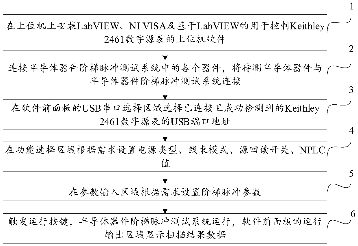
[0023] In order to make the object, technical solution and advantages of the present invention clearer, the implementation manner of the present invention will be further described in detail below in conjunction with the accompanying drawings.
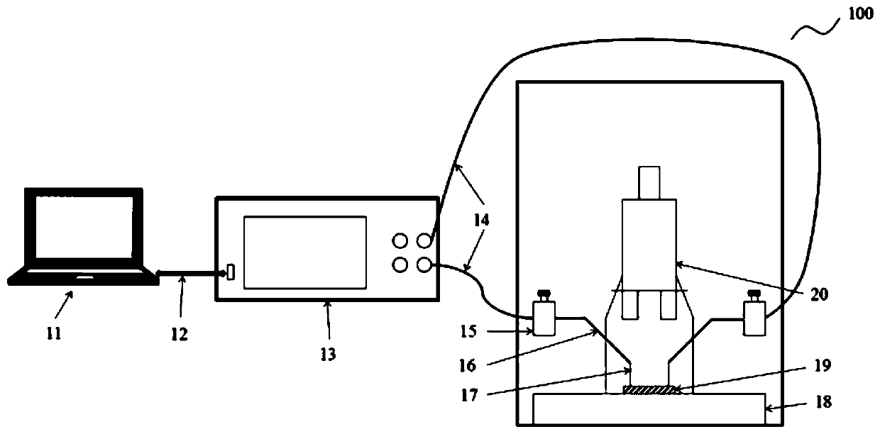
[0024] The embodiment of the present invention provides a semiconductor device step pulse test method based on LabVIEW, which is applied to such as figure 1 As shown in the semiconductor device step pulse test system, the semiconductor device step pulse test system 100 includes: a host computer 11, a Keithley 2461 digital source meter 13, a probe station base 18, a probe 17, a probe cover 16, and a probe magnetic base 15. Microscope 20.
[0025] The upper computer 11 is connected to the Keithley 2461 digital source meter 13 through the USB cable 12 that comes with the Keithley 2461 digital source meter 13, and the Keithley 2461 digital source meter 13 is connected to the probe magnetic base 15 through the BNC line 14, and the probe mag...
PUM
 Abstract
Description
Claims
Application Information