SRAM circuit yield analysis method based on non-Gaussian sampling

A technique of sampling distribution and Gaussian mixing, applied in electrical digital data processing, instrumentation, calculation, etc., can solve the problems of waste of sampling points and many iterations

Pending Publication Date: 2019-07-23
FUDAN UNIV
View PDF3 Cites 6 Cited by
  • Summary
  • Abstract
  • Description
  • Claims
  • Application Information

AI Technical Summary

Problems solved by technology

However μ * The initial value starts from 0, which makes the numb

Method used


Image

  • SRAM circuit yield analysis method based on non-Gaussian sampling
  • SRAM circuit yield analysis method based on non-Gaussian sampling
  • SRAM circuit yield analysis method based on non-Gaussian sampling

Examples


Embodiment Construction

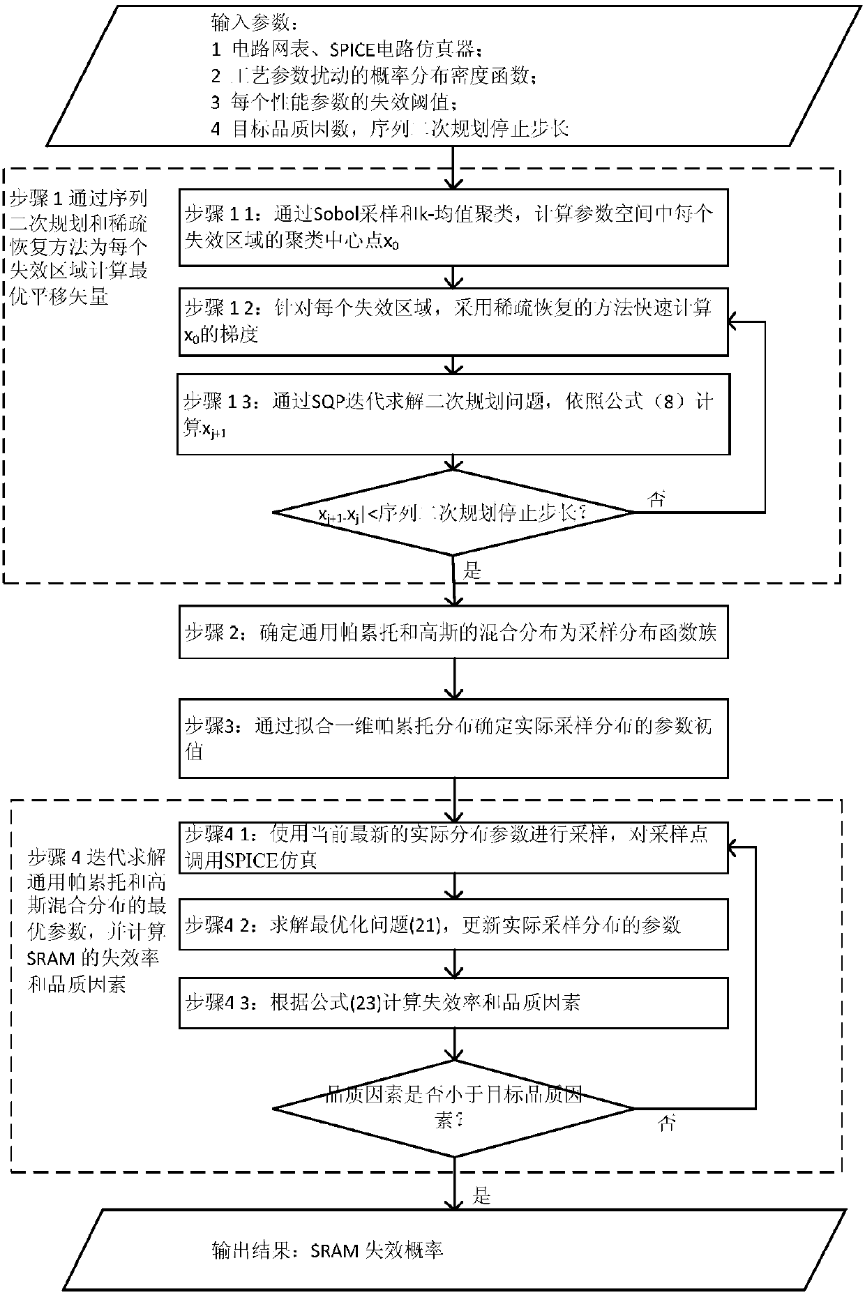
[0139] Now, the method of the present invention will be described through the implementation process of specific examples.

[0140] Implementation example 1

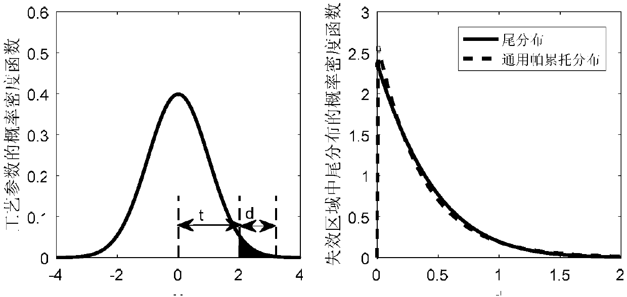
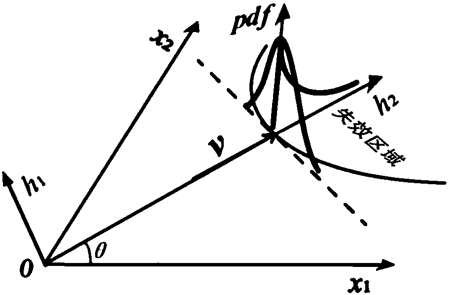
[0141] This example uses the Figure 5 circuit shown. Figure 5 It is a schematic diagram of an SRAM cell composed of 6 transistors under the 28nm process. In this example, the reading current I read as a performance indicator. The read current is defined as the current I on the two bit lines BL and I BL_ The difference between them directly affects the discharge speed of the bit line during the read operation. If the read current is less than a certain threshold, it is considered that the SRAM cell read failure.

[0142] Among the input parameters, the parameter space dimension D=6, and the target quality factor ρ=0.0865. The threshold voltages Vth1-Vth6 of the transistors M1-M6 in the circuit are disturbance process parameter variables.

[0143] In this example, the exact solution of the failure rate is 1.20e-...


PUM


Abstract

The invention belongs to the field of static random access memory circuit yield analysis in integrated circuit manufacturability design, and particularly relates to a method for obtaining an optimal actual sampling distribution parameter by adopting general Pareto and Gaussian joint distribution as an actual sampling distribution function family and minimizing cross entropy between actual samplingdistribution and ideal sampling distribution. The optimized actual sampling distribution is used for sampling and calculating the SRAM failure rate, so that the number of sampling points can be greatly reduced, and the sampling efficiency is improved. The key point of the invention lies in that general Pareto and Gaussian mixture distribution is adopted as a sampling distribution function family;aiming at the distributed parameter optimization problem, an iteration strategy is provided, sampling is continuously carried out, actual distribution parameters are updated, and the failure rate iscalculated until the failure rate meets the precision requirement. Experimental results show that the method provided by the invention is obviously superior to a method in the prior art.

Description

technical field [0001] The invention belongs to the field of Static Random Access Memory (SRAM) circuit yield analysis in integrated circuit manufacturability design, and specifically relates to a non-Gaussian sampling-based SRAM circuit yield analysis method. Background technique [0002] It is disclosed in the prior art that as the dimensions of semiconductor manufacturing processes continue to shrink, the influence of process disturbances on the performance and reliability of SRAM circuits becomes more and more significant. In order to reduce chip area, SRAM cells are often designed with the smallest process size, which makes their performance easily affected by process disturbances. At the same time, practice shows that a large number of repeated SRAM cells are included in an SRAM circuit. In order to ensure the yield rate of the overall SRAM circuit, the failure rate of each SRAM cell must be extremely low (generally should be lower than 10 -6 ). [0003] Generally, t...

Claims


Application Information

Patent Timeline
IPC IPC(8): G06F17/50
CPCG06F30/39G06F30/20
Inventor 曾璇严昌浩王胜国周海周电翟金源
Owner FUDAN UNIV
Why Eureka
Try Eureka