Integrated terahertz confocal imaging device and imaging method based on waveguide structure
A waveguide structure and imaging device technology, applied in the field of terahertz confocal imaging, can solve problems such as large volume and complex structure
- Summary
- Abstract
- Description
- Claims
- Application Information
AI Technical Summary
Problems solved by technology
Method used
Image
Examples
Embodiment 1
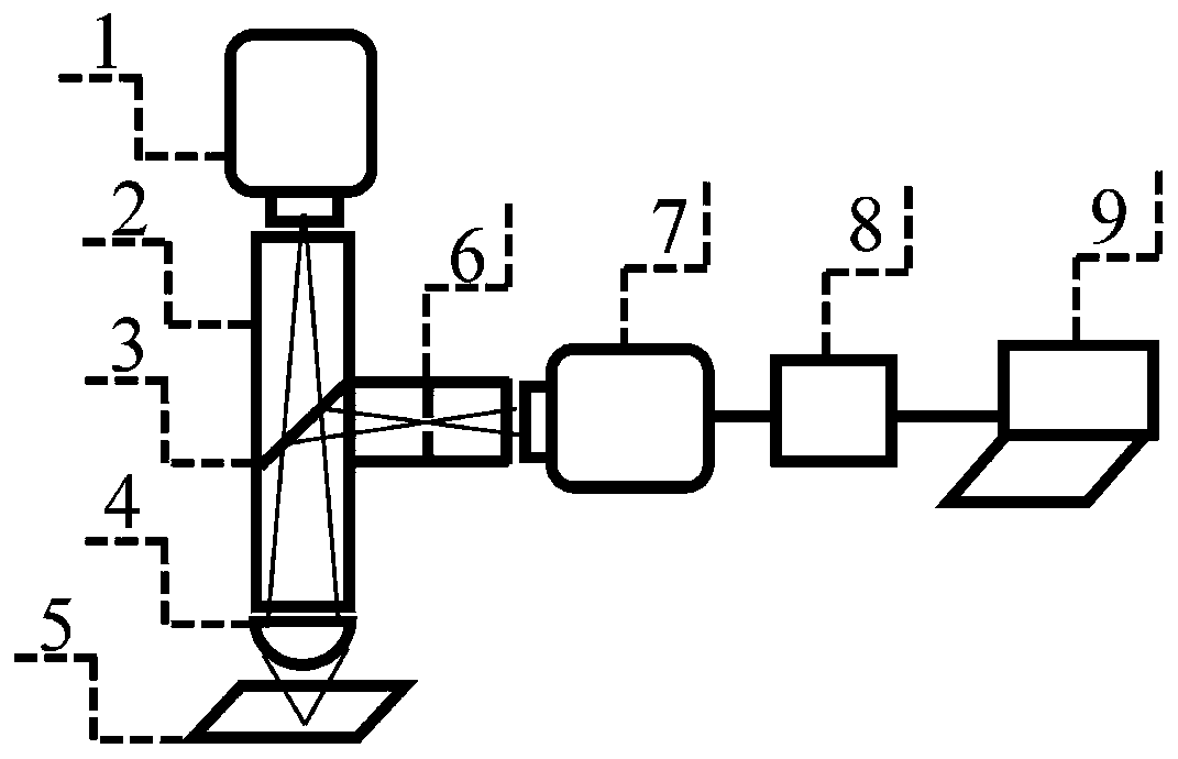
[0035] figure 1 It is a schematic diagram of an integrated terahertz confocal imaging device based on a waveguide structure, including a terahertz radiation source 1, a terahertz waveguide 2, a terahertz half-mirror 3, a terahertz focusing lens 4, an imaging sample 5, and a metal pinhole 6. Terahertz detector 7. Data acquisition card 8. Computer 9. The terahertz radiation source 1 is used to generate terahertz signals; the terahertz waveguide 2 is used to transmit terahertz waves to reduce the absorption of terahertz signals by water vapor in the air; the terahertz semi-transparent The half mirror 3 is placed in the terahertz waveguide at 45°, which can transmit and reflect terahertz signals; the terahertz focusing lens 4 can realize the function of focusing the incident terahertz waves; The imaging sample 5 is placed at the focal plane position after the terahertz wave is focused; the metal pinhole 6 is used to filter the terahertz signal reflected back from the imaging samp...
PUM
 Abstract
Description
Claims
Application Information


