Three-dimensional nonvolatile memory and manufacturing method thereof

A non-volatile, manufacturing method technology, applied in electric solid state devices, semiconductor devices, electrical components, etc., can solve problems such as memory cell interference, and achieve the effect of reducing interference

Active Publication Date: 2019-07-30
MACRONIX INT CO LTD
View PDF4 Cites 0 Cited by
  • Summary
  • Abstract
  • Description
  • Claims
  • Application Information

AI Technical Summary

Problems solved by technology

However, in the current operation of 3D NAND flash memory, the interference of memory cells is one of the main challenges in 3D NAND flash memory, especially the presence of trace residues

Method used


Image

  • Three-dimensional nonvolatile memory and manufacturing method thereof
  • Three-dimensional nonvolatile memory and manufacturing method thereof
  • Three-dimensional nonvolatile memory and manufacturing method thereof

Examples


Embodiment Construction

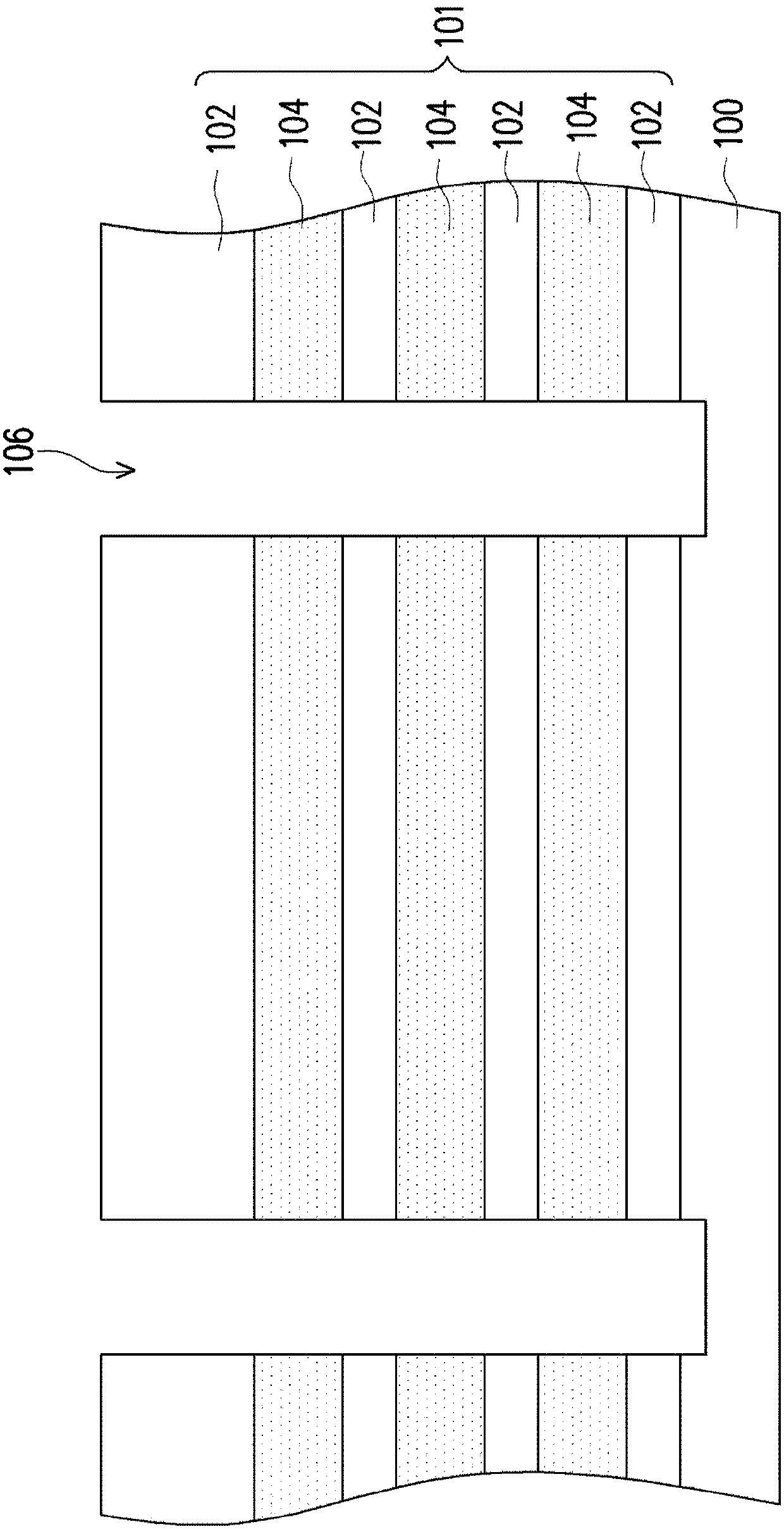
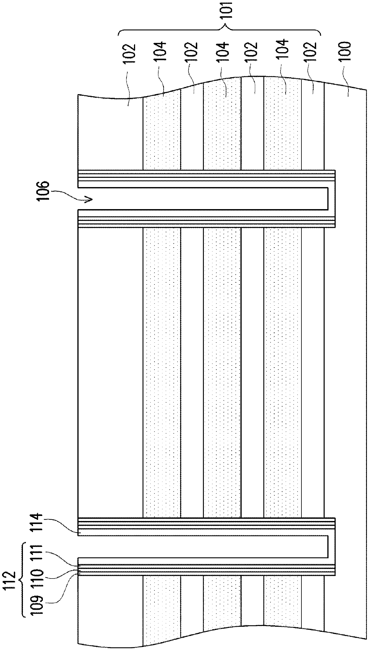
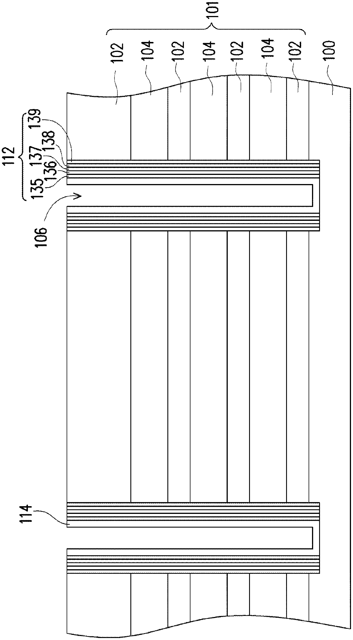
[0061] Figure 1A to Figure 1I It is a sectional view of the manufacturing process of the three-dimensional non-volatile memory according to some embodiments of the present invention. figure 2 for Figure 1B top view of .

[0062] Please refer to Figure 1A, forming a stacked structure 101 on the substrate 100 . The substrate 100 is, for example, a silicon substrate. In some embodiments, a doped region (eg, N+ doped region) (not shown) may be formed in the substrate 100 according to design requirements. The stacked structure 101 includes a plurality of insulating material layers 102 and a plurality of sacrificial layers 104 stacked alternately. The material of the insulating material layer 102 includes a dielectric material, such as silicon oxide. The material of the sacrificial layer 104 is different from that of the insulating material layer 102 , and has a sufficient etching selectivity ratio compared with the insulating material layer 102 , and is not particularly li...


PUM


Abstract

The invention relates to a three-dimensional nonvolatile memory and a manufacturing method thereof. The three-dimensional nonvolatile memory comprises a substrate, a charge storage structure, a laminated structure and a channel layer. The charge storage structure is disposed on the substrate. The laminated structure is arranged on one side of the charge storage structure and comprises a pluralityof insulating layers, a plurality of grids, a buffer layer and a barrier layer. The insulating layers and the gates are alternately stacked. The buffer layer is arranged between each grid and the charge storage structure and on the surface of the insulating layers. The barrier layer is arranged between each grid and the buffer layer. The end portion of the grid is protruded in a direction away from the channel layer with respect to the end portion of the barrier layer.

Description

technical field [0001] The present invention relates to a memory and its manufacturing method, and in particular to a three-dimensional non-volatile memory and its manufacturing method. Background technique [0002] The non-volatile memory element (eg, flash memory) has the advantage that the stored data will not disappear after power off, so it has become a memory element widely used in personal computers and other electronic devices. [0003] Flash memory arrays commonly used in the industry today include NOR flash memory and NAND flash memory. Because the structure of NAND flash memory is to connect each storage unit in series, its integration and area utilization are more efficient than NOR flash memory, so the storage density of NAND flash memory is much higher than that of NOR flash memory. Therefore, NAND flash memory has been widely used in various electronic products, especially in the field of mass data storage. [0004] In addition, in order to further improve t...

Claims


Application Information

Patent Timeline
Patent Type & Authority Applications(China)
IPC IPC(8): H01L27/1157H01L27/11578H01L21/28
CPCH01L29/40117H10B43/20H10B43/35
Inventor 林怡婷裘元杰李鸿志
Owner MACRONIX INT CO LTD
Why Eureka
Try Eureka