TOF image sensor demodulation pixel structure with rapid charge transfer

An image sensor and pixel demodulation technology, which is applied in the field of image sensors, can solve the problems of slow diffusion process, affecting the transfer speed of photoelectric charge, affecting the performance of PPD, etc., and achieve the effect of accelerating the transfer

Inactive Publication Date: 2019-08-09
TIANJIN UNIV
View PDF4 Cites 3 Cited by
  • Summary
  • Abstract
  • Description
  • Claims
  • Application Information

AI Technical Summary

Problems solved by technology

[0002] In the TOF image sensor demodulation pixel structure based on clamped photodiode (pinned photodiode, PPD), the photocharge transmission from PPD to FD node is controlled by the diffusion effect in the semiconductor, and the photocharge generated by PPD can only pass through the semiconductor. Diffusion is transferred, which seriously affects the transfer speed of photocharges, which limits the use of pixels at high modulation frequencies. Due to the slow diffusion process, it will affect the performance of PPD

Method used


Image

  • TOF image sensor demodulation pixel structure with rapid charge transfer
  • TOF image sensor demodulation pixel structure with rapid charge transfer

Examples


Embodiment Construction

[0012] The present invention will be described in further detail below in conjunction with the accompanying drawings and specific embodiments. It should be understood that the specific embodiments described here are only used to explain the present invention, not to limit the present invention.

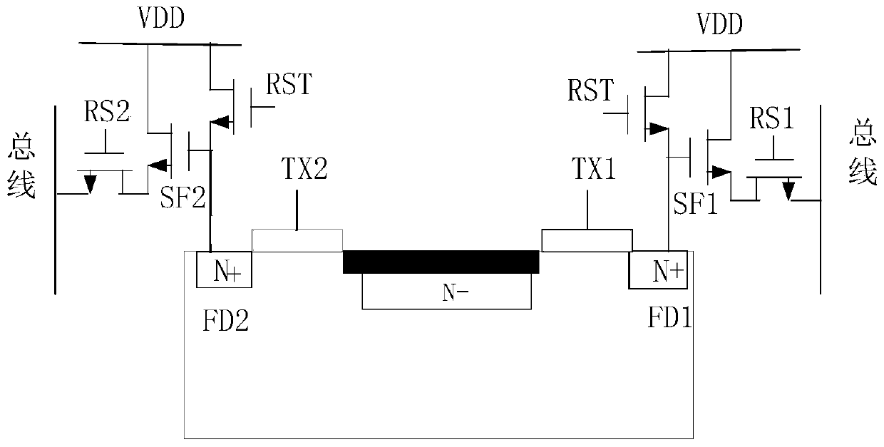
[0013] Such as figure 1 As shown, the existing PPD-based double floating diffusion node 4T pixel structure includes clamping photodiode PPD, transmission transistor (TX1, TX2), reset transistor RST, floating diffusion node (FD1, FD2), row gate Tubes (RS1, RS2) and source followers (SF1, SF2), floating diffusion nodes (FD1, FD2) are connected to clamp photodiodes PPD through transmission tubes (TX1, TX2), and are connected to source followers (SF1 , SF2), and the reset transistor RST connection, the reset transistor RST and the source follower (SF1, SF2) are connected to VDD, the source follower (SF1, SF2) and the row gating transistor (RS1, RS2), the row gating The tubes (RS1, RS2) ...


PUM


Abstract

The present invention discloses a TOF image sensor demodulation pixel structure with rapid charge transfer. The structure comprises a PPD-based dual-floating-diffusion-node 4T pixel unit which comprises two transfer tubes responsible for transferring photocharges from a PPD to double FD nodes and is characterized in that multiple adjacent polysilicon gates with a minimum width are employed by a gate of each of the transfer tubes, the multiple polysilicon gates are connected to a resistor array and are powered by the resistor array such that the polysilicon gates have increasing gate voltages,and the gate voltages are coupled to a semiconductor through a capacitor to form a lateral drift electric field. According to the invention, the gates of the polysilicon gates are substituted with multiple adjacent polysilicon gates with the minimum width, the increasing gate voltages are applied to the gates to form the lateral drift field of the photocharges under the gates of the transfer tubes, and the transfer of the photocharges is accelerated.

Description

technical field [0001] The invention relates to the technical field of image sensors, in particular to a demodulation pixel structure of a TOF image sensor with fast charge transfer. Background technique [0002] In the TOF image sensor demodulation pixel structure based on clamped photodiode (pinned photodiode, PPD), the photocharge transmission from PPD to FD node is controlled by the diffusion effect in the semiconductor, and the photocharge generated by PPD can only pass through the semiconductor. Diffusion is transferred, which seriously affects the transfer speed of photoelectric charges, which limits the use of pixels at high modulation frequencies. Due to the slow diffusion process, it will affect the performance of PPD. Some solutions obtain a larger photosensitive area by changing the shape of the device to increase the generation of photocharges; there are also solutions that increase the injection of impurities in the photosensitive area to optimize PDD performan...

Claims


Application Information

Patent Timeline
Patent Type & Authority Applications(China)
IPC IPC(8): H01L27/146
CPCH01L27/146H01L27/14601H01L27/14605
Inventor 高静牛洪星聂凯明徐江涛
Owner TIANJIN UNIV
Why Eureka
Try Eureka