Space vector pulse width modulation method and device
A technology of space vector pulse width and modulation method, applied in the field of three-level space vector pulse width modulation method and device, can solve the problems of harmonic characteristics, poor neutral point voltage balance suppression effect, underutilization of three-level, etc.
- Summary
- Abstract
- Description
- Claims
- Application Information
AI Technical Summary
Problems solved by technology
Method used
Image


Examples
Embodiment 1
[0180] As attached figure 1 Shown is the main circuit topology of an NPC three-level inverter (ie, converter 10). Attached figure 1 In, the inverter output AC voltage is realized by controlling the on and off state of the three-phase bridge arm switch tube. Taking the A-phase output as an example, the corresponding relationship between the A-phase output terminal voltage and the on-state of the switch is shown in Table 1 below (where 1 means on and 0 means off).
[0181] Table 1 Correspondence between A-phase output terminal voltage and switch on state
[0182]
[0183] Similarly, phases B and C also have the same switch state corresponding relationship described above.
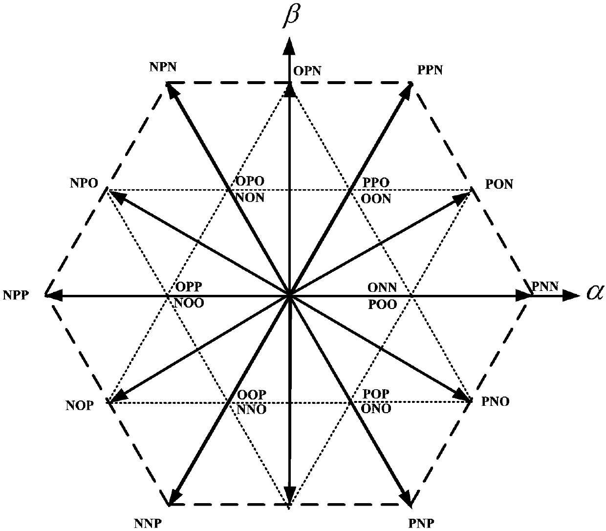
[0184] Therefore, in the three-level inverter circuit of the converter 10, there are three switching states of each phase: -U dc / 2(N), 0(O), U dc / 2(P). For a three-phase symmetric system, a total of 3 3 = 27 switch states, each switch state corresponds to a basic (voltage space) vector, as attached figure 2...
Embodiment 2
[0293] As attached Figure 5 As shown, a specific embodiment of a space vector pulse width modulation device used for modulation of a converter 10 includes:
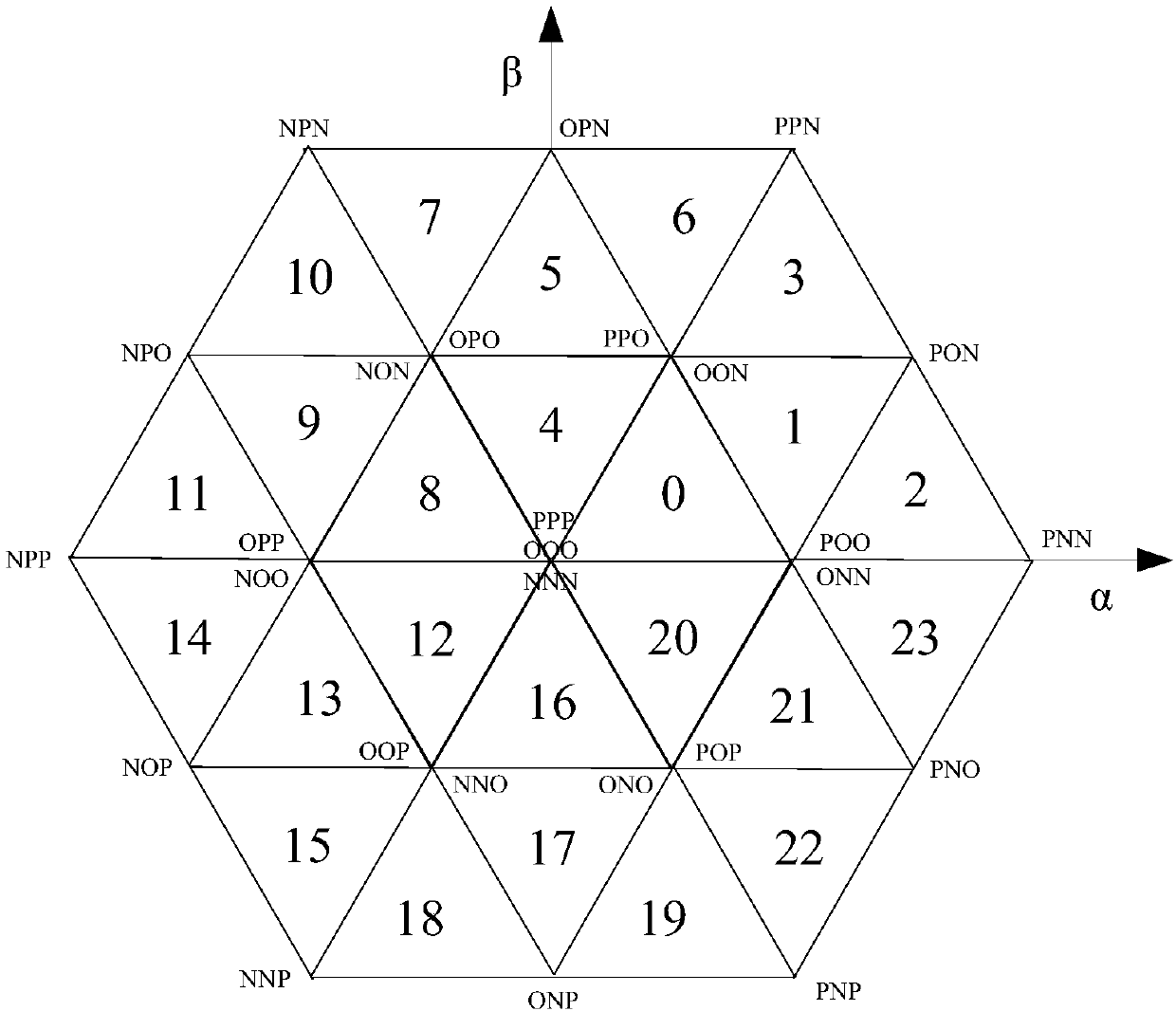
[0294] Sector judging unit 1, judging the reference voltage vector The sector
[0295] Triangular area judgment unit 2, according to the reference voltage vector Reference voltage vector for judgment of the sector in which it is located The triangular area in which it is located;
[0296] The basic vector action time calculation unit 3, according to the reference voltage vector It is in the triangular area, calculated to synthesize the reference voltage vector The action time of each basic vector;
[0297] The basic vector fitting arrangement unit 4, according to the redundant vector pair in the basic vector, make full use of s / 2 is axisymmetric distribution, and the zero vector is T s / 4 is axisymmetric distribution, and the basic vector fitting arrangement is performed, T s Is the switching period of the three-phase bridg...
PUM
 Abstract
Description
Claims
Application Information
 - R&D
- Intellectual Property
- Life Sciences
- Materials
- Tech Scout
- Unparalleled Data Quality
- Higher Quality Content
- 60% Fewer Hallucinations
Browse by: Latest US Patents, China's latest patents, Technical Efficacy Thesaurus, Application Domain, Technology Topic, Popular Technical Reports.
© 2025 PatSnap. All rights reserved.Legal|Privacy policy|Modern Slavery Act Transparency Statement|Sitemap|About US| Contact US: help@patsnap.com