A method and device for manufacturing a high aspect ratio micro-nano structure

A micro-nano structure and manufacturing device technology, applied in the direction of micro-structure devices, manufacturing micro-structure devices, micro-structure technology, etc., can solve the problems of cumbersome process and difficult adjustment of thickness-to-width ratio, and achieve simple operation, simple and clear principle, and easy operation convenient effect

Active Publication Date: 2022-03-29
HUAZHONG UNIV OF SCI & TECH
View PDF7 Cites 0 Cited by
  • Summary
  • Abstract
  • Description
  • Claims
  • Application Information

AI Technical Summary

Problems solved by technology

Nowadays, in the surface treatment of nanoimprinting, photolithography, inkjet printing and other technologies, micro-nano structures with high aspect ratios have high application value, but for this kind of micro-nano structures that are not easy to manufacture, how to quickly and effectively The manufacture of the
[0003] At present, the hydrophobic coating on the surface of the substrate and the nano-pattern on the surface of the substrate are mostly used to realize the high-thickness-width-ratio micro-nano structure. Due to different ink material systems, there are different material coatings and micro-nano pattern processing, the process is cumbersome, and the thickness-width ratio is difficult to control.

Method used


Image

  • A method and device for manufacturing a high aspect ratio micro-nano structure
  • A method and device for manufacturing a high aspect ratio micro-nano structure
  • A method and device for manufacturing a high aspect ratio micro-nano structure

Examples


Embodiment 1

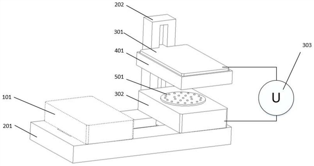
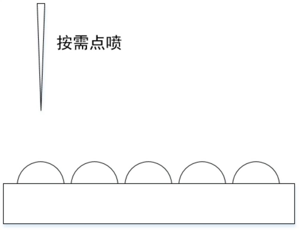
[0035] figure 2 It is a structural schematic diagram of Embodiment 1 of the high-thickness ratio micro-nano structure manufacturing device, Figure 3-6 is to use figure 1 Schematic diagram of the process flow for the device to complete the fabrication of high aspect ratio micro-nano structures.

[0036] This embodiment functionally includes a motor movement module, a micro-nano structure manufacturing module and a curing module. The motor movement module can control the Y-axis and Z-axis movement, the Y-axis motor is installed in the base 201, and the Z-axis motor is installed in the column 202; the upper electrode plate 301 can be controlled by the Z-axis motor to move up and down in the chute, and the lower electrode plate 302 can be controlled by the Y-axis motor to move left and right in the chute, and the two are connected to the external high-voltage amplifier system 303; the UV curing lamp lampshade 401 is connected to the external chute of the column, and can be man...

Embodiment 2

[0047] Figure 7 A second embodiment of the device of the invention is given. Most of the structures of the device described in Embodiment 2 are the same as those described in Embodiment 1, except that the structures of the upper electrode plate 301 and the lower electrode plate 302 are different.

[0048] The upper electrode plate 301 of embodiment 2 is evenly divided into four sub-electrode plates 30101, such as Figure 8 As shown, each electrode plate is respectively connected to 4 channels of 2 DC high-voltage amplifiers in the external high-voltage amplification system 303, and the voltage regulation of each small electrode plate on the upper electrode plate 301 can be realized simultaneously through computer software, and the upper electrode plate 301 can be simultaneously adjusted. The electrode plate 301 is made of hard plastic as a whole, and the small electrode plates are placed in the frame, and insulators are used to block between the small electrode plates. Accor...


PUM


Abstract

The invention discloses a method and device for manufacturing a micro-nano structure with a high aspect ratio, which belongs to the field of flexible electronic manufacturing. The method specifically includes: applying an electric field to the printed micro-nano droplet pattern on the substrate, inducing the edge of the micro-nano droplet pattern to shrink laterally and stretch longitudinally to form a micro-nano structure with a high aspect ratio. The device includes an upper electrode plate, a lower electrode plate and an external high-voltage amplifier system. The wire connection ends of the upper electrode plate and the lower electrode plate are respectively connected to the external high-voltage amplifier system. The substrate that has been printed with micro-nano droplet patterns is placed on the lower On the electrode plate, an external high-voltage amplifier system is activated to form an electric field between the upper and lower electrode plates, which induces the lateral shrinkage of the micro-nano droplet pattern edge and longitudinal stretching to form a high aspect ratio micro-nano structure. The invention generates micro-nano patterns with high aspect ratios through electric field induction, significantly improves the manufacturing efficiency of the micro-nano structures, and meets precision requirements.

Description

technical field [0001] The invention relates to the field of flexible electronics manufacturing, in particular to a method and device for manufacturing a micro-nano structure with a high aspect ratio. Background technique [0002] With the development of science and technology, the demand for refined equipment is getting stronger and stronger. Flexible electronic technology has broad application prospects in micro-nano processing, especially in the fields of sensors, flexible displays, and smart skin. Nowadays, in the surface treatment of nanoimprinting, photolithography, inkjet printing and other technologies, micro-nano structures with high aspect ratios have high application value, but for this kind of micro-nano structures that are not easy to manufacture, how to quickly and effectively The manufacture of it becomes a difficult problem that needs to be solved. [0003] At present, hydrophobic coatings on the substrate surface and nano-patterns on the substrate surface a...

Claims


Application Information

Patent Timeline
Patent Type & Authority Patents(China)
IPC IPC(8): B81C1/00
CPCB81C1/00031B81C1/00634
Inventor 徐洲龙刘振东陈建魁吴学洲王培琳
Owner HUAZHONG UNIV OF SCI & TECH
Why Eureka
Try Eureka