NVMe SSD PCIe data packet analysis method based on FPGA

A parsing method and data packet technology, which are applied in the field of FPGA-based NVMeSSDPCIe packet parsing, can solve the problems of complex PCIe packet parsing process and many logic resources, and achieve the effects of complete functions, saving logical resources, and simplifying parsing process.

Active Publication Date: 2019-08-16
HARBIN INST OF TECH
View PDF3 Cites 2 Cited by
  • Summary
  • Abstract
  • Description
  • Claims
  • Application Information

AI Technical Summary

Problems solved by technology

[0004] The purpose of the present invention is to solve the problem that the traditional PCIe data packet parsing process is complex and needs to occupy too many logical resources, and a FPGA-based NVMe SSD PCIe data packet parsing method is proposed

Method used


Image

  • NVMe SSD PCIe data packet analysis method based on FPGA
  • NVMe SSD PCIe data packet analysis method based on FPGA
  • NVMe SSD PCIe data packet analysis method based on FPGA

Examples


specific Embodiment approach 1

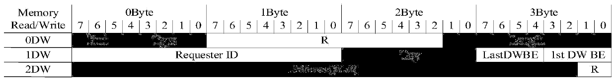
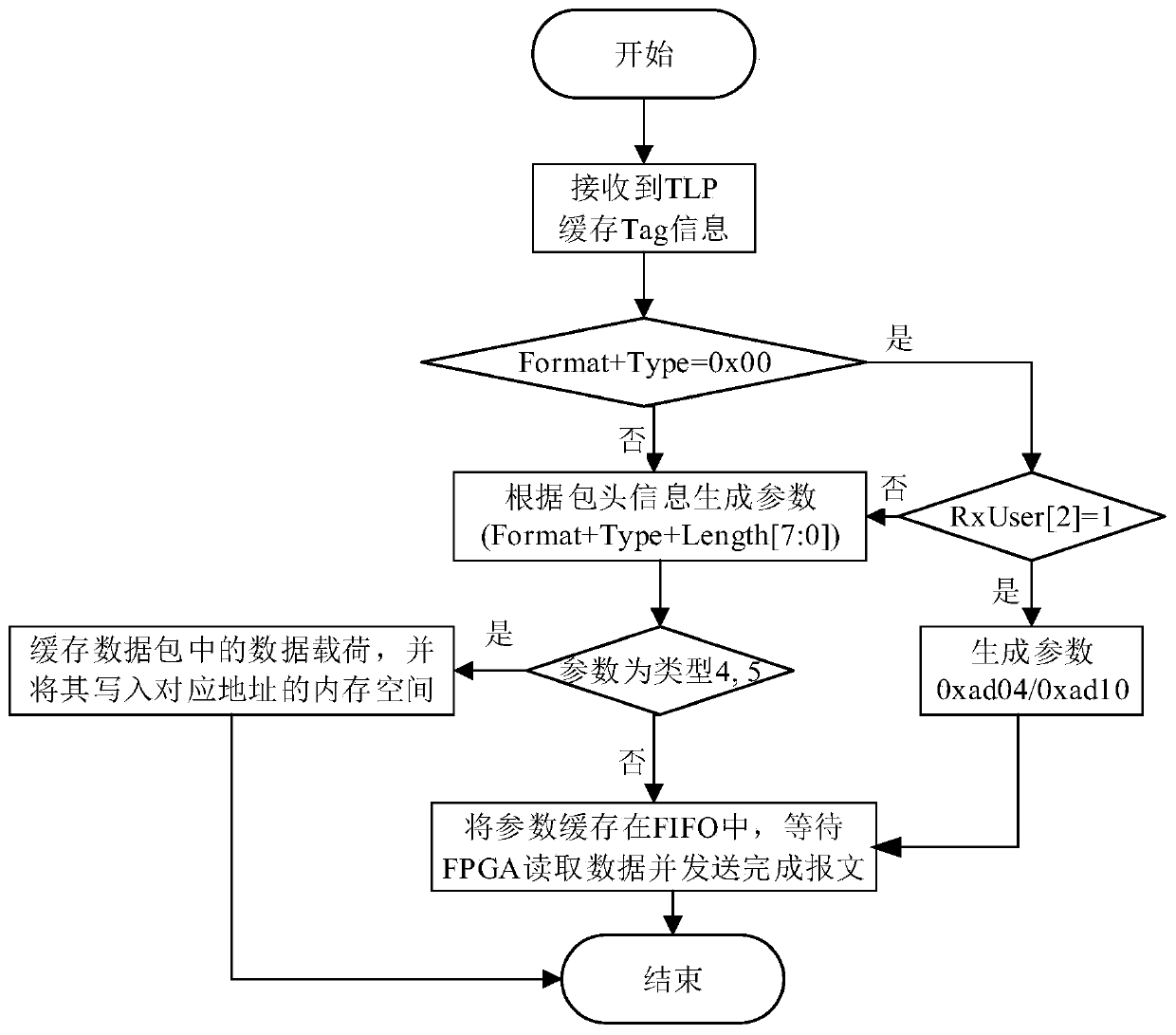
[0026] Specific embodiment one: a kind of FPGA-based NVMe SSD PCIe data packet analysis method described in this embodiment, the TLP (transaction layer data packet) that needs to analyze in the described FPGA-based NVMe SSD PCIe data packet analysis method includes reading memory (Memory Read) TLP and write memory (Memory Write) TLP; and for each TLP, its corresponding format (Format) information, type (Type) information and length (Length) information need to be parsed;

[0027] Wherein: the format information and the type information are used to determine the type of the corresponding TLP, and the length information is used to determine the function of the corresponding TLP;

[0028] The TLP parameter of each TLP is a 16-bit binary number, the upper 8 bits of the TLP parameter are the format information and type information of the corresponding TLP, and the lower 8 bits of the TLP parameter are the lower 8 bits of the length information of the corresponding TLP.

[0029] The...

specific Embodiment approach 2

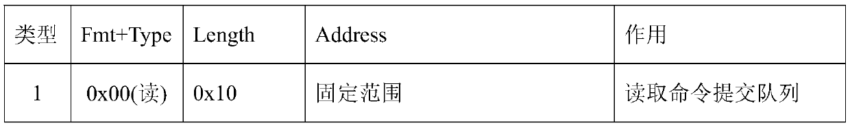
[0041] Embodiment 2: The difference between this embodiment and Embodiment 1 is that the TLP parameters include 5 types; the TLP parameters of Type 1 are expressed as 0x0010, the TLP parameters of Type 2 are expressed as 0x0010 or 0x0004, and the TLP parameters of Type 3 are expressed as 0x0010 or 0x0004. The parameter is represented as 0x0040, the TLP parameter of type 4 is represented as 0x4020, and the TLP parameter of type 5 is represented as 0x4004.

[0042] Each type of TLP parameter in this embodiment is generated by combining the lower 8-bit information of the format, type and length.

specific Embodiment approach 3

[0043] Embodiment 3: This embodiment is different from Embodiment 2 in that: the type 2 TLP parameter representation is replaced with 0xad04 / 0xad10, and 0xad04 / 0xad10 is used to distinguish it from the type 1 TLP parameter.

[0044] The present invention defines "TLP parameters" as follows:

[0045] (1) The parameter is a 16-bit binary number;

[0046] (2) The upper 8 bits of the parameter are the Fmt+Type of the TLP, and the lower 8 bits of the parameter are the Length[7:0] of the TLP;

[0047] (3) The TLP parameter of special definition type 2 is 0xad04 / 0xad10.

[0048] The present invention has carried out special definition to the TLP parameter of type 2, and its reason is as follows: TLP type 1, 3, 4 and 5 correspond to a kind of TLP parameter respectively, and type 2 corresponds to two kinds of Fmt+Type+Length parameters, wherein a kind of parameter 0x0010 is the same as the TLP parameter of type 1.

[0049] In order to simplify the parsing process, the present invent...


PUM


Abstract

The invention discloses an NVMe SSD PCIe data packet analysis method based on an FPGA, belonging to the technical field of storage. The invention solve the problems that a traditional PCIe data packetanalysis process is complex, and too many logic resources need to be occupied. By means of the characteristics of the TLP parameters of the received NVMe data packet and the change rule of the address, the data packet analysis process is simplified, and the type and the effect of the TLP packet can be accurately judged under the condition that the TLP address is not analyzed. The FIFO cache module formed by the Block Ram in the FPGA only needs to record the TLP parameters and the number fields. Compared with a traditional data analysis method, the simplification method provided by the invention can save 57% of logic resources while ensuring the function integrity of the data analysis module without recording the address of the TLP. The invention can be applied to the technical field of storage.

Description

technical field [0001] The invention belongs to the technical field of storage, and in particular relates to an FPGA-based NVMe SSD PCIe data packet parsing method. Background technique [0002] High-speed data storage devices are widely used in areas such as radar testing. In order to improve the read and write speed of storage devices, reduce the size and power consumption of devices, and adapt to the development trend of miniaturization and compactness, the emerging NVMe (Non-Volatile Memory express, non-volatile memory host controller) in the storage field can be used Interface Specification) SSD (Solid State Drive) to build a portable high-speed storage device, the read and write speed of this SSD can be as high as 2GB / s or more. The performance of the storage device implemented by Zynq (ARM+FPGA) and NVMeSSD is limited by the main frequency and threads of the ARM core, while the storage device implemented by FPGA and NVMe SSD can make better use of the read and write ...

Claims


Application Information

Patent Timeline
Patent Type & Authority Applications(China)
IPC IPC(8): G06F13/40G06F13/42
CPCG06F13/4022G06F13/4221G06F2213/0026
Inventor 张京超刘旺孟凡廓朱凯晖乔立岩彭喜元
Owner HARBIN INST OF TECH
Why Eureka
Try Eureka