Circuit board punching device for applicant electronics

A technology that applies electronics and circuit boards. It is applied in metal processing and other directions. It can solve problems such as adverse effects, inconvenient use by users, and complicated operations, and achieve the effect of meeting the requirements of use and convenient and quick punching.

Inactive Publication Date: 2019-08-23
JIANGSU INST OF ECONOMIC & TRADE TECH
View PDF7 Cites 0 Cited by
  • Summary
  • Abstract
  • Description
  • Claims
  • Application Information

AI Technical Summary

Problems solved by technology

[0002] In the process of PCB board production, a punching machine is usually used for punching. The more common technical means are to punch it manually with a mold. Although this method is relatively simple and the operation process is relatively mature, it has a great impact on the factory. Production cost input, manpower input, etc., all have adverse effects
[0003] The so-called electronic circuit board punching device is a device that converts potential energy with the help of related components during the production process of electronic components, converts elastic potential energy into kinetic energy of the blade, and then punches the circuit board into holes. The main method of punching circuit boards in the factory production line is to use electric drills to drill holes. This method has a slow hole forming speed and complicated operation, which makes it very inconvenient for users to use at this stage.

Method used


Image

  • Circuit board punching device for applicant electronics
  • Circuit board punching device for applicant electronics
  • Circuit board punching device for applicant electronics

Examples


Embodiment Construction

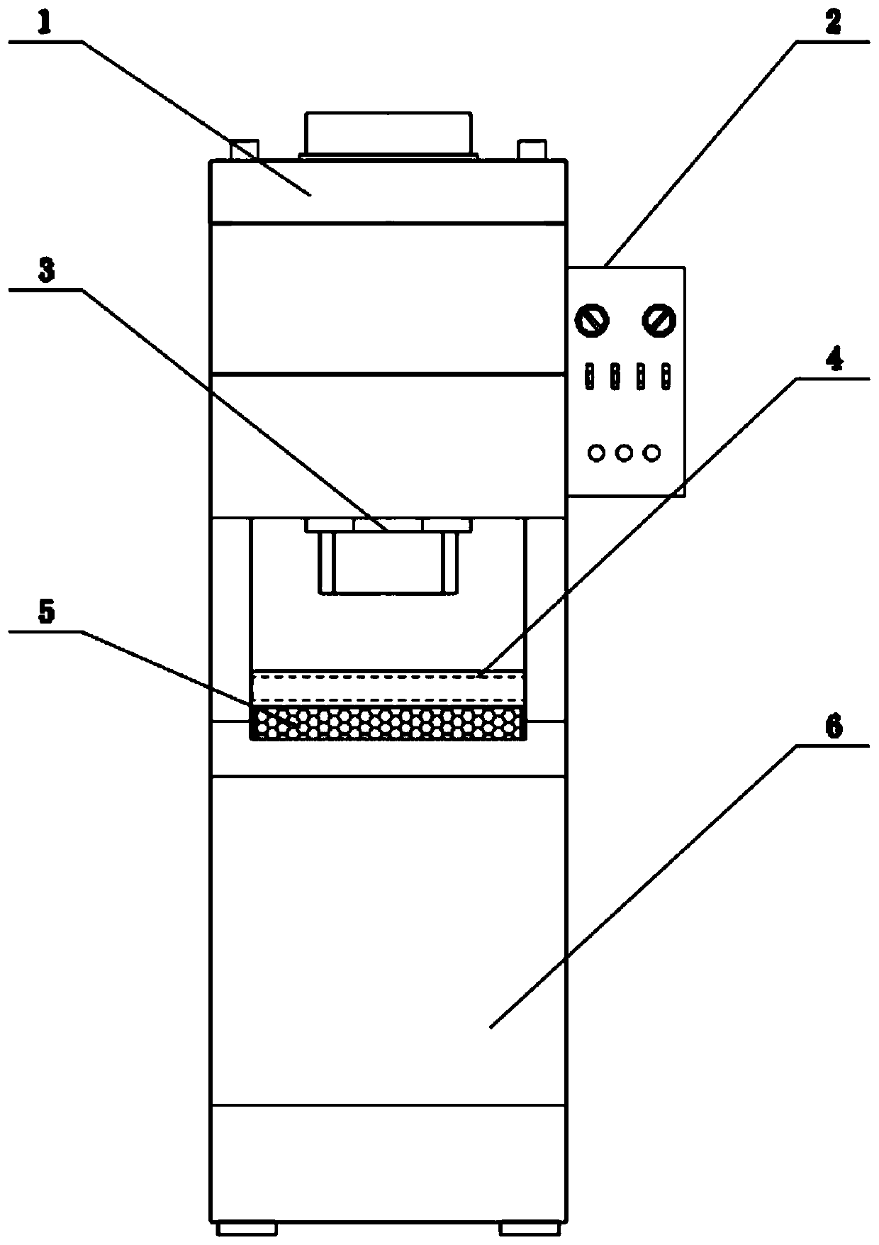
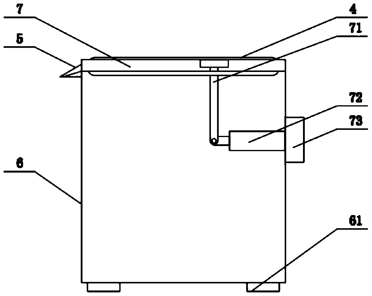
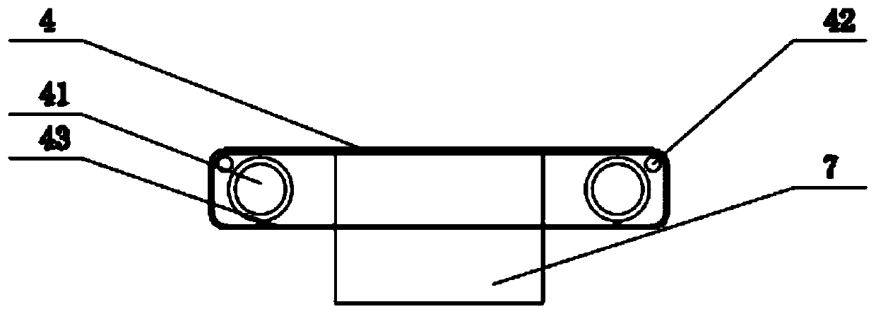
[0021] see Figure 1-Figure 6 As shown, the technical solution adopted in this specific embodiment is: it includes a hydraulic mechanism 1, a control box 2, a stamping mechanism 3, a transmission device 4, a discharge plate 5, a base 6, and an air pressure mechanism 7; A stamping mechanism 3 is arranged below, and the stamping mechanism 3 is movably installed above the base 6, the control box 2 is installed on the right side of the hydraulic mechanism 1, the transmission device 4 is set on the top of the base 6, and the discharge plate 5 is set on the top of the transmission device 4. In the front, the air pressure mechanism 7 is fixedly installed on the rear side of the base 6. The air pressure mechanism 7 includes a steering rod 71, a telescopic rod 72, a fixed seat 73, and a punching plate 74; one end of the telescopic 72 is connected with the fixed seat 73 , the other end of telescoping rod 72 is flexibly connected with the bottom of steering rod 71, and the top of steerin...


PUM


Abstract

The invention discloses a circuit board punching device for applicant electronics, and relates to the technical field of circuit board processing. The device comprises a hydraulic mechanism, a controlbox, a stamping mechanism, a conveying device, a discharge plate, a base and an air pressure mechanism; the stamping mechanism is arranged below the hydraulic mechanism, the stamping mechanism is movably arranged above the base, the control box is arranged on the right side of the hydraulic mechanism, the conveying device is arranged on the top of the base, the discharge plate is arranged in front of the conveying device, the air pressure mechanism is fixedly arranged on the rear side of the base, and the air pressure mechanism comprises a steering rod, a telescopic rod, a fixed seat and a punching plate; and one end of the telescopic rod is connected with the fixed seat, the other end of the telescopic rod is movably connected with the bottom of the steering rod, and the fixed seat is connected with the right side surface of the base through a bolt. The circuit board punching device for applicant electronics has the beneficial effects that the flow type integrated design is adopted in the working process, energy is saved, environment is protected, pollution is avoided, punching is convenient and fast, and the use requirement on applicant electronics is met.

Description

technical field [0001] The invention relates to the technical field of circuit board processing, in particular to a circuit board punching device for applied electronics. Background technique [0002] In the process of PCB board production, a punching machine is usually used for punching. The more common technical means are to punch it manually with a mold. Although this method is relatively simple and the operation process is relatively mature, it has a great impact on the factory. Production cost input, manpower input, etc., all have adverse effects. [0003] The so-called electronic circuit board punching device is a device that converts potential energy with the help of related components during the production process of electronic components, converts elastic potential energy into kinetic energy of the blade, and then punches the circuit board into holes. The main method of punching circuit boards in the factory production line is to use electric drills to drill holes....

Claims


Application Information

Patent Timeline
Patent Type & Authority Applications(China)
IPC IPC(8): B26F1/40B26D7/06B26D7/00
CPCB26D7/00B26D7/0625B26F1/40
Inventor 张亮
Owner JIANGSU INST OF ECONOMIC & TRADE TECH
Why Eureka
Try Eureka