Method for manufacturing liquid crystal panel

A technology for liquid crystal panels and manufacturing methods, applied in the fields of nonlinear optics, instruments, optics, etc., which can solve the problems of cutting margin liquid crystal panel miniaturization obstacles, difficulty in using the first glass substrate and the second glass substrate, etc., and achieve reduction Effect of stock removal

Pending Publication Date: 2019-08-23
DISCO CORP
View PDF7 Cites 0 Cited by
  • Summary
  • Abstract
  • Description
  • Claims
  • Application Information

AI Technical Summary

Problems solved by technology

[0005] However, in the above-mentioned processing method of cutting the first glass substrate and the second glass substrate with a cutting tool, it is necessary to set a cutting allowance of at least 1 mm according to the thickness of the cutting tool, so it is difficult to say that the first and second glass substrates can be fully utilized. 1 glass substrate and 2nd glass substrate
In addition, there is also a problem that the large cutting allowance remaining on the outer side of the sealing tape is likely to be an obstacle to miniaturization of the liquid crystal panel.

Method used


Image

  • Method for manufacturing liquid crystal panel
  • Method for manufacturing liquid crystal panel
  • Method for manufacturing liquid crystal panel

Examples


Embodiment Construction

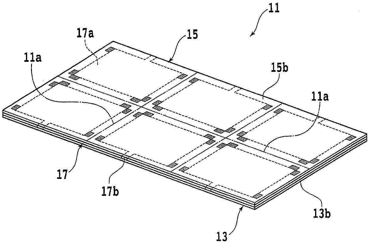
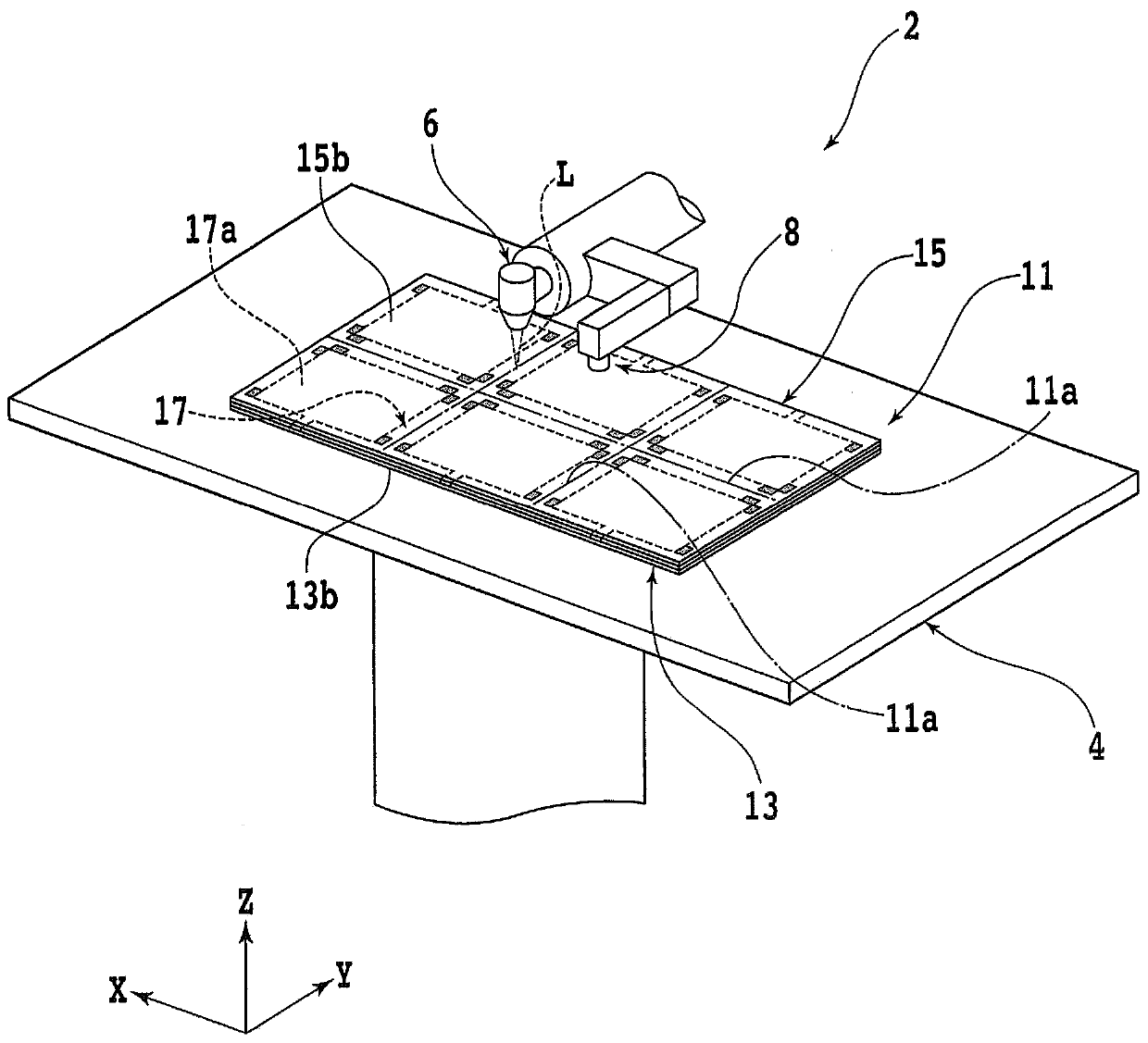
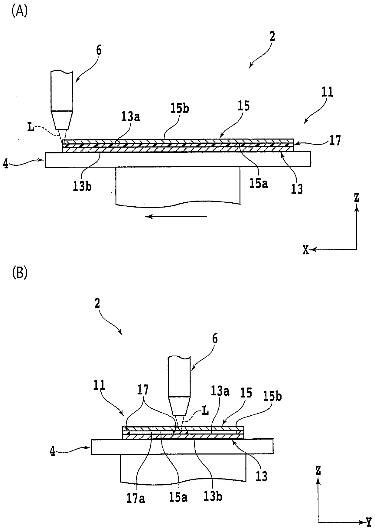
[0019] An embodiment of one embodiment of the present invention will be described with reference to the drawings. The manufacturing method of the liquid crystal panel of this embodiment comprises a laser processing step (refer to figure 2 , image 3 of (A), image 3 of (B), Figure 4 (A) and Figure 4 (B)) and segmentation steps (see Figure 5 ).

[0020] In the laser processing step, the laser beam of the wavelength transmitted through the glass substrate is condensed inside the bonded substrate to form a shield tunnel including fine holes and modified parts surrounding the fine holes in the bonded substrate. It has: a sealing tape that defines a liquid crystal chamber; and two glass substrates that are bonded together through the sealing tape. In the dividing step, the bonded substrate is divided into a plurality of liquid crystal panels along the shield tunnel formed on the bonded substrate. Hereinafter, the manufacturing method of the liquid crystal panel of this e...


PUM


Abstract

Provided is a method for manufacturing a liquid crystal panel to reduce the amount of cutting when the liquid crystal panel is cut out from a bonded substrate. A method for manufacturing a liquid crystal panel comprises processing a bonded substrate to produce a plurality of liquid crystal panels, the bonded substrate comprising: a sealing tape dividing a plurality of liquid crystal chambers, andtwo glass substrates attached to each other through the sealing tape. The method for manufacturing the liquid crystal panel includes a laser processing step of positioning the condensed region of a laser beam passing through the wavelength of the glass substrates inside the bonded substrate and between two adjacent liquid crystal chambers while irradiating the laser beam along the sealing strip, and forming a shield tunnel including pores and a modified portion surrounding the pores in the bonded substrate; and a dividing step of along the shield tunnel formed on the bonded substrate, dividingthe bonded substrate into a plurality of liquid crystal panels.

Description

technical field [0001] The invention relates to a method for manufacturing a liquid crystal panel. Background technique [0002] A liquid crystal display device used as a monitor of electronic equipment has a liquid crystal panel that is an array substrate on which a TFT (Thin Film Transistor: Thin Film Transistor) for driving liquid crystals is formed and a color filter on which a color filter is provided. It is formed by laminating the light sheet substrate. A sealing tape made of resin or the like is provided between the array substrate and the color filter substrate, and liquid crystals are sealed in liquid crystal cells divided by the sealing tape. [0003] For the above-mentioned liquid crystal panel, for example, after bonding the first glass substrate to be divided into a plurality of array substrates and the second glass substrate to be divided into a plurality of color filter substrates through a sealing tape, the The bonded substrates (hereinafter referred to as...

Claims


Application Information

Patent Timeline
Patent Type & Authority Applications(China)
IPC IPC(8): G02F1/1333
CPCG02F1/133351G02F1/1339G02F1/1303
Inventor 桐原直俊
Owner DISCO CORP
Why Eureka
Try Eureka