Lens adjustment structure and light transmitting device thereof
A light-emitting device and a technology for adjusting the structure, which is applied in the field of optical communication and can solve problems such as the inability to meet the spacing requirements between signal channels
- Summary
- Abstract
- Description
- Claims
- Application Information
AI Technical Summary
Problems solved by technology
Method used
Image
Examples
Embodiment approach 1
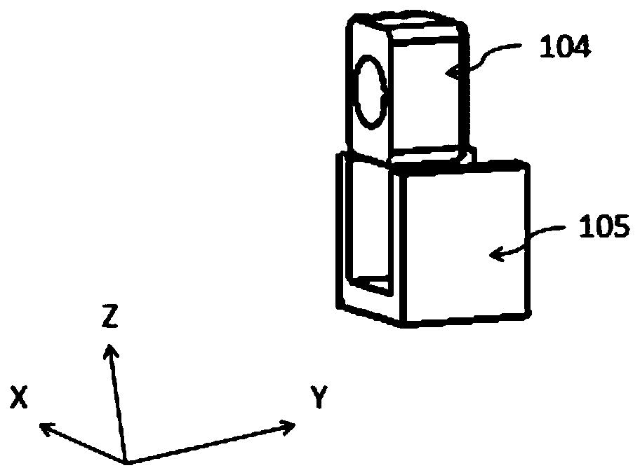
[0025] Such as Image 6 The shown lens adjustment structure of the present invention, the lens adjustment structure is divided into two pieces, and is composed of the lens adjustment structure upper part 205 and the lens adjustment structure lower part 206. The lower end surface of the lens adjustment structure upper part 205 is an inclined plane, and the lens adjustment structure lower part 206 has a slope matching the lower end surface of the lens adjustment structure upper part 205, the lens adjustment structure upper part 205 and the lens adjustment structure lower part 206 contact through the slope surface, the top of the lens adjustment structure is provided with a lens 104, and the lens adjustment structure is connected with the lens 104 in the horizontal direction movement to realize the adjustment of the lens 104 in the X-axis and Y-axis directions; the upper part 205 of the lens adjustment structure moves up and down along the slope of the lower part 206 of the lens a...
Embodiment approach 2
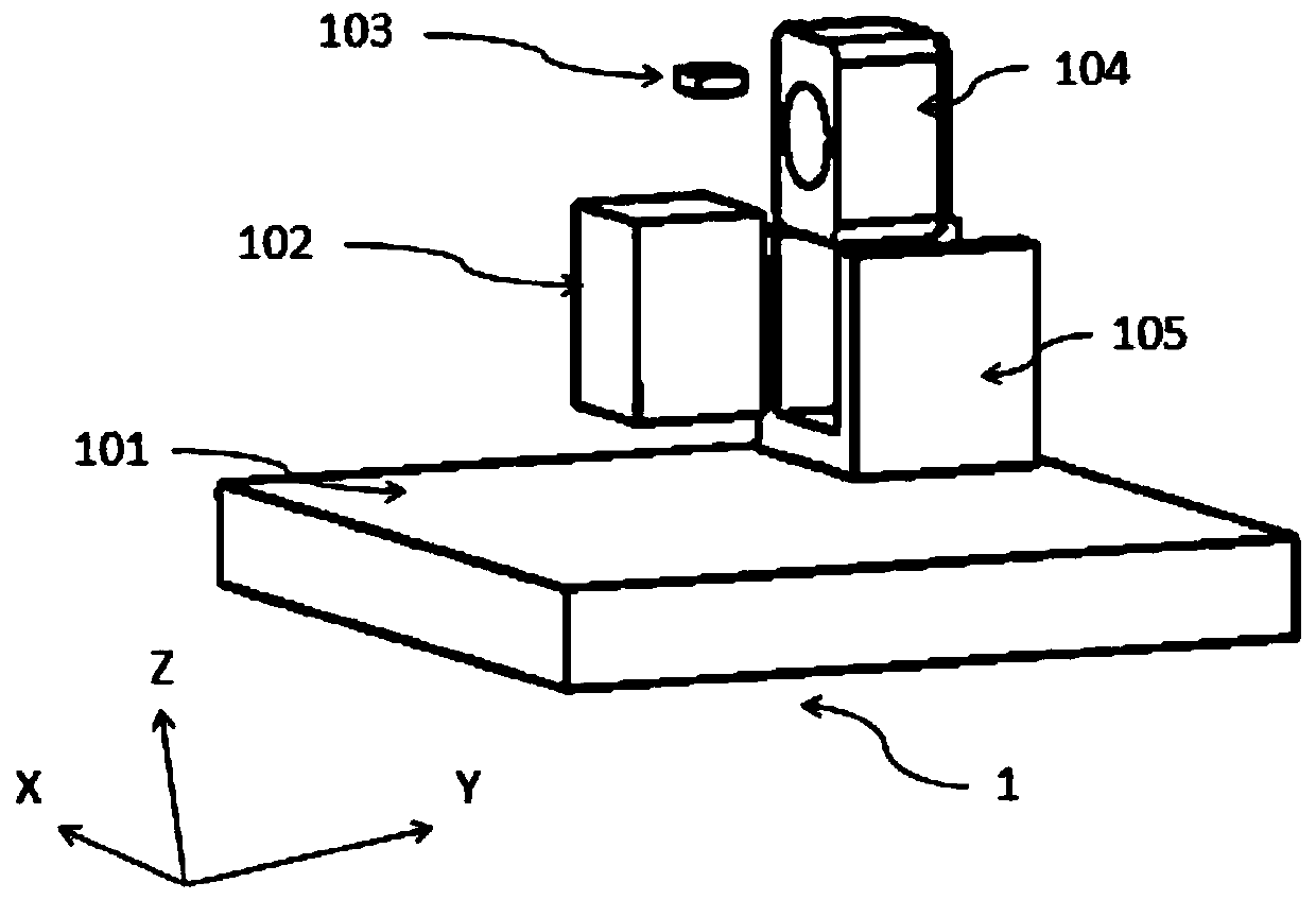
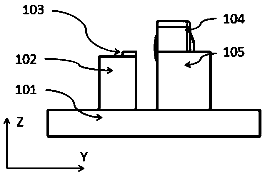
[0027] Such as Figure 7-9 The light-emitting device of a signal channel unit that adopts the lens adjustment structure of the present invention is shown based on a carrier substrate 101, a heat sink 102 is arranged on the signal channel unit, a semiconductor laser chip 103 is arranged on the top of the heat sink 102, and a semiconductor laser chip 103 is arranged on the top of the heat sink 102. The laser chip 103 is used as a light source for emitting modulation signals. The heat sink 102 is used to make the position of the semiconductor laser chip 103 reach a specific height and play a role in heat dissipation. The lens adjustment structure in Embodiment 1 is also provided. The top of the lens adjustment structure The provided lens 104 is used to convert the light emitted by the semiconductor laser chip 103 into parallel light or converging light, and the heat sink 102 and the lens adjustment structure are sequentially arranged on the carrier substrate 101 along the light pa...
Embodiment approach 3
[0029] Such as Figure 10-11 The light-emitting device of the multi-signal channel unit that adopts the lens adjustment structure of the present invention as shown is based on a carrier base
[0030] Based on the board 101, several signal channel units described in Embodiment 2 are arranged in parallel on its upper part, and the center-to-center distance a of the semiconductor laser chips of two adjacent signal channel units is equal. At present, the distance between the signal channels of the light-emitting device is usually less than 1mm, but it can also be set to a width different from the existing calculation, and the lens width b is usually 0.7mm, but it can also be set to a different width from the existing calculation, because the present invention The light-emitting device in the embodiment adopts the lens adjustment structure in Embodiment 1, so it can meet the requirement that the distance between signal channels is less than 1mm, realize the parallel mode of multipl...
PUM
 Abstract
Description
Claims
Application Information
 - R&D
- Intellectual Property
- Life Sciences
- Materials
- Tech Scout
- Unparalleled Data Quality
- Higher Quality Content
- 60% Fewer Hallucinations
Browse by: Latest US Patents, China's latest patents, Technical Efficacy Thesaurus, Application Domain, Technology Topic, Popular Technical Reports.
© 2025 PatSnap. All rights reserved.Legal|Privacy policy|Modern Slavery Act Transparency Statement|Sitemap|About US| Contact US: help@patsnap.com


