Breaking apparatus, breaking method and breaking plate

A technology for cutting devices and substrates, applied in the direction of welding/welding/cutting items, electrical components, circuits, etc., can solve problems such as inability to perform good cutting and chip shapes that do not meet specifications

Pending Publication Date: 2019-08-27
MITSUBOSHI DIAMOND IND CO LTD
View PDF2 Cites 0 Cited by
  • Summary
  • Abstract
  • Description
  • Claims
  • Application Information

AI Technical Summary

Problems solved by technology

[0009] Due to the need for miniaturization of the chip, etc., in the case of cutting a bonded substrate with solder balls having a small distance between the solder balls and the planned cutting position in the manner disclosed in Patent Document 1, sometimes the The middle cutting rod comes into contact with the solder balls, which prevents good cutting (segmentation of the substrate), and abnormalities such as the shape of the chip after cutting does not meet the specifications.

Method used


Image

  • Breaking apparatus, breaking method and breaking plate
  • Breaking apparatus, breaking method and breaking plate
  • Breaking apparatus, breaking method and breaking plate

Examples


Embodiment Construction

[0020]

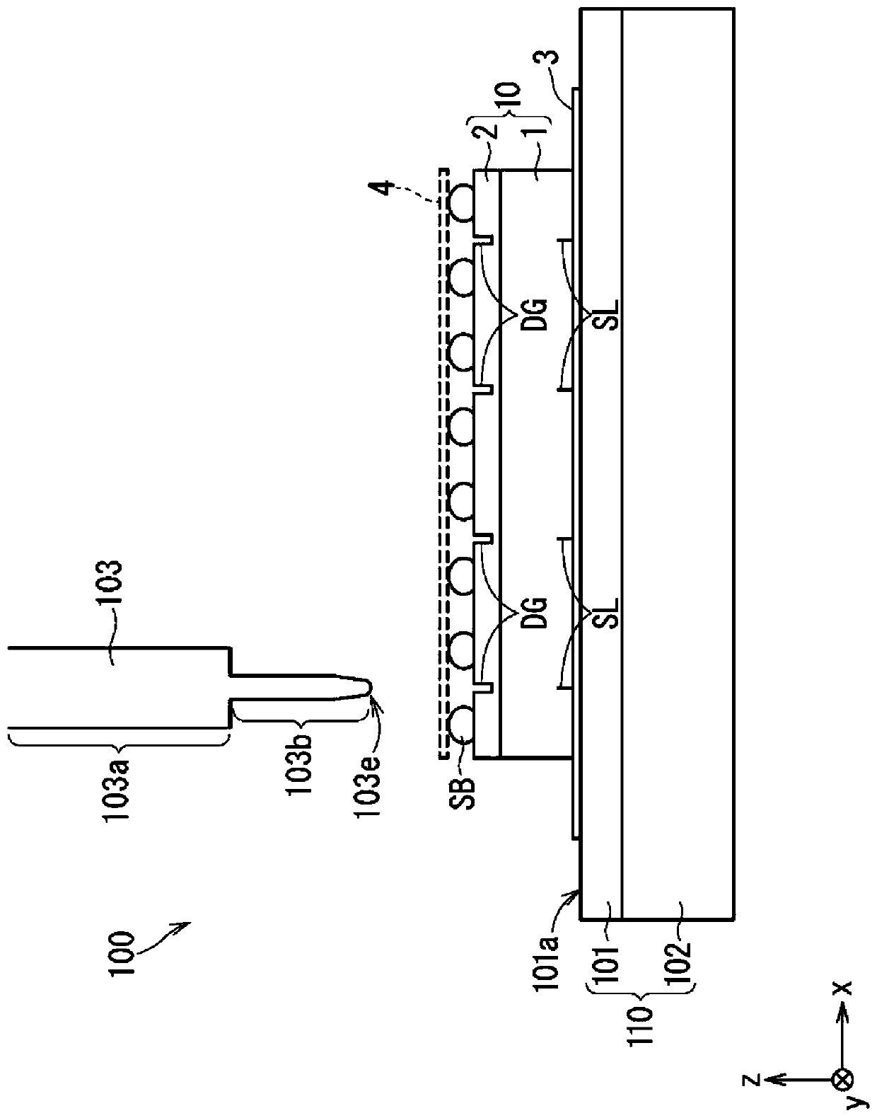
[0021] figure 1 It is a figure which schematically shows the state of cutting the bonded board|substrate 10 using the cutting apparatus 100 of this embodiment.

[0022] The bonded substrate 10 is, for example, a single substrate as a whole bonded by bonding the first substrate 1 and the second substrate 2 made of a brittle material. As the first substrate 1 , in addition to substrates (glass substrates) made of various glasses such as borosilicate glass, alkali-free glass, and alkali glass such as soda glass, a ceramic substrate is also exemplified. As the second substrate 2 , in addition to the silicon substrate, a thermosetting resin substrate is exemplified. In the following description, the first substrate 1 is a glass substrate and the second substrate 2 is a silicon substrate. The first substrate 1 is only described as the glass substrate 1 and the second substrate 2 is only described as the silicon substrate 2 .

[0023] Furthermore, in this embodiment, if ...


PUM

PropertyMeasurementUnit
hardnessaaaaaaaaaa

Abstract

The invention provides a breaking apparatus capable of appropriately breaking a substrate with solder balls. The invention is an apparatus for breaking a substrate with a plurality of solder balls onone main surface thereof along a groove portion provided on the one main surface, and the apparatus has a stage carrying the substrate in a horizontal posture by taking one side of the one main surface as an upper side; and a breaking plate which is arranged to be freely lifted up and lowered down in a vertical posture in which a blade at one end portion becomes a lower end portion and which is pressed into the substrate from a state in which the blade abuts against the groove portion so as to break the substrate at a position where the groove portion is formed. In the breaking plate, the blade portion including the blade extends from one end portion of the base portion having a predetermined thickness and is set to be narrower than the base portion. The thickness of the blade portion is twice smaller than the minimum value of the distance between the center of the cross section of the groove portion when the breaking plate is pressed in and the solder balls.

Description

technical field [0001] The present invention relates to cutting of a substrate provided with solder balls on one main surface. Background technique [0002] As one of semiconductor chips having a structure in which a silicon substrate layer and a glass substrate layer are bonded via an adhesive layer, there is a semiconductor chip having solder balls on the silicon substrate layer. As a method of manufacturing such a semiconductor chip, a scribe line is formed at a planned cutting position on the glass substrate side of a bonded substrate obtained by bonding a silicon substrate and a glass substrate through an adhesive layer, and a cutting plan is formed on the silicon substrate side. After forming the groove portion (dicing groove) reaching the adhesive layer, solder balls are formed at predetermined positions on the silicon substrate, and after such solder balls are formed, cutting (break) is performed, and between the scribed line and the dicing groove It is a known tech...

Claims


Application Information

Patent Timeline
Patent Type & Authority Applications(China)
IPC IPC(8): H01L21/304H01L21/78H01L21/67
CPCH01L21/304H01L21/78H01L21/67011H01L21/67092H01L21/67121H01L24/742H01L24/81H01L24/11H01L24/12H01L24/75B23K2101/42B23K2103/52
Inventor 村上健二田村健太荣田光希武田真和
Owner MITSUBOSHI DIAMOND IND CO LTD
Why Eureka
Try Eureka