Touch display module and electronic equipment
A touch display and touch technology, which is applied in electrical digital data processing, character and pattern recognition, instruments, etc., can solve the problems of light energy loss, reduce the success rate of fingerprint recognition under the screen, etc., and achieve high sensitivity and accuracy. Effect
Active Publication Date: 2019-08-30
BOE TECH GRP CO LTD +1
12 Cites 1 Cited by
AI-Extracted Technical Summary
Problems solved by technology
[0004] The purpose of the present invention is to provide a touch display module and electronic equipment, which are used to solve the problem that the base of the touch substrate easily affects the polarization state of the passing light during the fin...
Method used
Based on the existence of the above-mentioned problems, the inventors of the present invention have found through research that the root cause of the reduction in light energy is that there is an uncertain phase difference in the base 401 in the touch substrate 40, therefore, by setting the touch substrate 40 The phase difference of the substrate 401 and/or the angle between the slow axis of the substrate 401 and the absorption axis of the polarizing structure 30 reduces or eliminates the loss of light energy generated by the substrate 401, so as to improve the sensitivity and accuracy of the entire identification system. Spend.
[0044] According to the specific structure and actual application process of the above-mentioned touch display module, in the touch display module provided by the embodiment of the present invention, by setting the base of the touch substrate to have a preset phase difference, the display panel can be emitted The difference between the energy of the first light and the energy of the second light incident on the fingerprint identification module is not greater than the threshold, so that the lo...
Abstract
The invention discloses a touch display module and electronic equipment, and relates to the technical field of optical fingerprint identification, for solving the problems that in the fingerprint identification process, a substrate of a touch substrate easily affects the polarization state of passing light, so that optical energy loss is generated when the light is emitted to a fingerprint identification receiving end through a polarizer and the success rate of fingerprint identification under a screen is reduced. The touch display module comprises a touch substrate located on the light emitting side of a display panel, wherein the base of the touch substrate has a preset phase difference, so as to enable the difference between the energy of the first light ray emitted by the display paneland the energy of the second light ray entering a fingerprint recognition module to be not larger than a threshold value, wherein the second light ray is a light ray which is irradiated to the fingerprint recognition module after the first light ray is reflected by an external object and then penetrates through the polarizing structure, the touch substrate and the display panel. The touch displaymodule provided by the invention is used for realizing a touch display function.
Application Domain
Character and pattern recognitionInput/output processes for data processing
Technology Topic
PolarizerFingerprint recognition +5
Image
Examples
- Experimental program(1)
Example Embodiment
[0033] In order to further illustrate the touch display module and electronic equipment provided by the embodiments of the present invention, a detailed description will be given below in conjunction with the accompanying drawings.
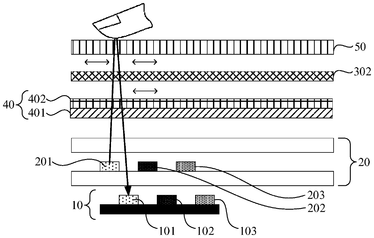
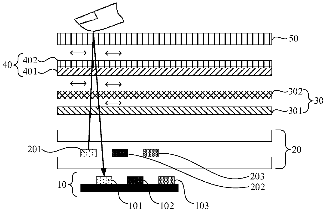
[0034] like figure 1 As shown, in the related art, the optical under-display fingerprint identification system includes a fingerprint identification module 10, a display panel 20, a polarizing structure 30 (including a 1/4 wave plate 301 and a linear polarizing plate 302), The touch substrate 40 and the cover 50 , wherein the fingerprint recognition module 10 is located on the non-light emitting side of the display panel 20 , and the polarizing structure 30 , the touch substrate 40 and the cover 50 are located on the light emitting side of the display panel 20 .
[0035] When the above-mentioned optical under-screen fingerprint identification system performs fingerprint identification, the light-emitting unit in the display panel 20 is used as a light source, and the light emitted by the light source is irradiated to the touch fingerprint through the polarizing structure 30, the touch control substrate 40 and the cover plate 50. , after being reflected by the fingerprint, the reflected light passes through the cover plate 50, the touch substrate 40 and the polarizing structure 30 to the display panel 20 in sequence, and passes through the imaging aperture provided in the display panel 20, and then enters the fingerprint identification module 10. After the recognition module 10 receives the reflected light, it forms a pattern of a fingerprint for subsequent comparison and recognition.
[0036] In more detail, the above-mentioned polarizing structure 30 may include a circular polarizer, and the light emitted by the light source passes through the circular polarizer and becomes linearly polarized light, and the polarization direction of the linearly polarized light is parallel to the transmission axis of the circular polarizer; the linearly polarized light When continuing to pass through the touch substrate 40, due to the phase difference in the base 401 of the touch substrate 40, the linearly polarized light will become elliptically polarized light; after the half-wave loss of the fingerprint reflection, the reflected light is still elliptically polarized The light rotates in the opposite direction; when the reflected light passes through the touch substrate 40 again, affected by the phase difference of the base 401 of the touch substrate 40, the polarization state of the reflected light changes, and the reflected light with the changed polarization state passes through the circular polarizer again , only the component parallel to the transmission axis of the circular polarizer can pass through, resulting in a reduction in the light energy received by the fingerprint recognition module 10 and a reduction in the sensitivity and accuracy of the entire recognition system.
[0037] Based on the existence of the above problems, the inventors of the present invention have found through research that the root cause of the reduction in light energy is that there is an uncertain phase difference in the base 401 of the touch substrate 40. Therefore, by setting the base 401 of the touch substrate 40 The phase difference and/or the angle between the slow axis of the substrate 401 and the absorption axis of the polarizing structure 30 reduces or eliminates the loss of light energy caused by the substrate 401, so as to improve the sensitivity and accuracy of the entire identification system.
[0038] An embodiment of the present invention provides a touch display module, including: a display panel, a polarizing structure located on the light-emitting side of the display panel, and a fingerprint identification module located on the non-light-emitting side of the display panel. include:
[0039] The touch substrate located on the light-emitting side of the display panel, the base of the touch substrate has a preset phase difference, so that the difference between the energy of the first light emitted by the display panel and the energy of the second light incident on the fingerprint recognition module is not greater than a threshold value, Wherein, the second light is the light that is reflected by the first light by an external object and passes through the polarizing structure, the touch control substrate and the display panel and irradiates the fingerprint identification module.
[0040] Specifically, in the above-mentioned touch display module, the fingerprint identification module is arranged on the non-light-emitting side of the display panel, and the polarizing structure and the touch substrate are arranged on the light-emitting side of the display panel, and the above-mentioned touch display module also includes setting On the cover plate on the light emitting side of the display panel, the polarizing structure and the touch substrate should be arranged between the display panel and the cover plate. The above-mentioned display panel includes a plurality of light emitting units, and the fingerprint identification module includes a plurality of fingerprint identification units corresponding to the plurality of light emitting units, and each light emitting unit is provided with an imaging small corresponding only to the light emitting unit. After being reflected by the fingerprint of the touching finger, the first light emitted by each light-emitting unit will pass through the small hole corresponding to the light-emitting unit and be received by the fingerprint recognition unit corresponding to the light-emitting unit in the fingerprint recognition module, thereby Realize the fingerprint identification function.
[0041] like figure 2 As shown, for example, the display panel includes a red light emitting unit 201, a green light emitting unit 202 and a blue light emitting unit 203, and the fingerprint recognition module 10 includes a red fingerprint recognition unit 101 corresponding to the red light emitting unit 201, and a green light emitting unit 202 The corresponding green fingerprint identification unit 102 and the blue fingerprint identification unit 103 corresponding to the blue light emitting unit 203 , the light emitted by the red light emitting unit 201 is received by the red fingerprint identification unit 101 after being reflected by the fingerprint.
[0042] When the above touch display module actually performs fingerprint recognition, the specific process is as follows:
[0043] The light-emitting unit in the display panel emits the first light, and the finger touches the surface of the cover plate facing away from the display panel. The first light emitted by the light-emitting unit passes through the touch substrate, the polarizing structure and the cover plate, and then shoots to the touch panel. finger, the light is reflected by the fingerprint of the touch finger to form a reflected second light, which is received by the corresponding fingerprint recognition unit in the fingerprint recognition module after passing through the cover, touch substrate, polarizing structure and display panel , so as to realize the fingerprint identification function.
[0044]According to the specific structure and actual application process of the above-mentioned touch display module, in the touch display module provided by the embodiment of the present invention, by setting the base of the touch substrate to have a preset phase difference, it is possible to make the first output from the display panel The difference between the energy of the light and the energy of the second light incident on the fingerprint identification module is not greater than the threshold, thereby reducing or eliminating the loss of light energy caused by the substrate, and improving the sensitivity and accuracy of the entire identification system.
[0045] In some embodiments, the above-mentioned touch substrate can be arranged between the display panel and the polarizing structure.
[0046] Specifically, when the touch substrate is arranged between the display panel and the polarizing structure, the fingerprint identification process of the touch display module includes:
[0047] The light-emitting unit in the display panel emits the first light, and the finger touches the surface of the cover plate facing away from the display panel. The first light emitted by the light-emitting unit passes through the touch substrate, the polarizing structure and the cover plate in sequence, and then shoots to the touch panel. The light is reflected by the fingerprint of the touch finger to form a reflected second light. The second light passes through the cover plate, polarized light structure, touch substrate and display panel in turn and is recognized by the corresponding fingerprint in the fingerprint recognition module. The unit receives it, so as to realize the fingerprint identification function.
[0048] It can be seen that when the touch substrate is arranged between the display panel and the polarizing structure, the first light rays pass through the polarizing structure and the cover plate and are irradiated to the touch finger, and then the second light is reflected by the finger, and the second light is compatible with the finger The received first light has the same polarization state, but the vibration direction is opposite, so the second light reflected by the finger can all pass through the polarizing structure without loss of light energy. Moreover, when the light continues to pass through the touch substrate When the substrate is used, it is only possible to change the polarization state of the second light without affecting the light energy of the second light. Therefore, when the above-mentioned touch substrate is arranged between the display panel and the polarizing structure, the light energy loss of the transmitted light due to the phase difference of the substrate is avoided.
[0049] like figure 2 As shown, in some embodiments, the polarizing structure 30 provided in the above embodiments includes a linear polarizer 302 ; the base 401 of the touch control substrate 40 includes a 1/4 wave plate.
[0050] Specifically, in the case where the touch substrate 40 is disposed between the display panel 20 and the polarizing structure 30, the polarizing structure 30 can further be configured to include a linear polarizer 302, and the base 401 of the touch substrate 40 includes a 1/4 wave plate, Under this structure, the fingerprint identification process of the touch display module includes:
[0051] The light emitting unit in the display panel 20 emits the first light, and the finger touches the surface of the cover plate 50 facing away from the display panel 20, and the first light emitted by the light emitting unit sequentially passes through the 1/4 wave plate (that is, the touch substrate 40 base 401), the linear polarizer 302 and the cover plate 50, and shoot to the finger where the touch occurs. At this time, the first light received by the finger is linearly polarized light, and the polarization direction of the linearly polarized light is the same as that of the linear polarizer 302. The transmission axes are parallel; the first ray is reflected by the fingerprint of the touching finger to form a reflected second ray, and the second ray passes through the cover plate 50, the linear polarizer 302, the 1/4 wave plate and the display panel 20 in turn, and is captured by the fingerprint The corresponding fingerprint identification unit in the identification module 10 receives it, thereby realizing the fingerprint identification function. It should be noted that since the second light is still linearly polarized light, and the polarization direction of the second light is still parallel to the transmission axis of the linear polarizer 302, but the vibration direction is opposite to the linear polarization direction of the first light received by the finger, Therefore, when the second light is transmitted to the fingerprint identification unit, when passing through the linear polarizer 302, the light energy will not be absorbed by the linear polarizer 302, so that the fingerprint identification module 10 can receive all of the second light reflected by the fingerprint. light energy.
[0052] In the above setting, the touch substrate 40 is located between the display panel 20 and the polarizing structure 30, and the polarizing structure 30 includes a linear polarizer 302, and the base 401 of the touch substrate 40 includes a 1/4 wave plate, which not only makes the touch substrate 40 The phase difference of the base 401 will not cause the loss of the light energy of the second light, which ensures the accuracy of the fingerprint identification of the display module. Moreover, the above-mentioned setting method enables the base 401 of the touch substrate 40 to weaken the impact on the display panel 20. The reflection effect generated by the second light further improves the success rate and accuracy of fingerprint recognition by the display module.
[0053] In addition, setting the polarizing structure 30 as a linear polarizer 302 better reduces the production cost of the display module compared to setting the polarizing structure 30 as a circular polarizer in the prior art.
[0054] It is worth noting that the base 401 of the above-mentioned touch substrate 40 can directly use the existing 1/4 wave plate, or can use the material actually required by the base 401, and by setting appropriate parameters, the base 401 with the function of a 1/4 wave plate can be produced. . Exemplarily, the phase difference of the substrate 401 of the touch substrate 40 is set to be between 100nm and 160nm, and the angle between the slow axis of the substrate 401 of the touch substrate 40 and the absorption axis of the linear polarizer 302 is 45° or 135°. °.
[0055] Specifically, when manufacturing the base 401 of the touch control substrate 40 , the phase difference of the base 401 is set between 100 nm˜160 nm, so that the base 401 has the function of a 1/4 wave plate. In addition, the angle between the slow axis of the base 401 of the touch substrate 40 and the absorption axis of the linear polarizer 302 can be set according to actual needs. The angle between the absorption axes of the sheet 302 is 45° or 135°, and when the angle between the slow axis of the substrate 401 and the absorption axis of the linear polarizer 302 is 45° or 135°, the The reflective effect of the display panel 20 on the second light is more conducive to improving the success rate and accuracy of fingerprint recognition by the display module.
[0056] like image 3 As shown, in some embodiments, the touch substrate 40 can be set on the side of the polarizing structure 30 facing away from the display panel 20; the angle between the slow axis of the base 401 of the touch substrate 40 and the absorption axis of the polarizing structure 30 90° or 0°.
[0057] Specifically, when the angle between the slow axis of the base 401 of the touch substrate 40 and the absorption axis of the polarizing structure 30 is 90°, the first light and the second light can only pass through the slow axis of the base 401; When the angle between the slow axis of the substrate 401 of the control substrate 40 and the absorption axis of the polarizing structure 30 is 0°, the first light and the second light can only pass through the fast axis of the substrate 401, therefore, when the touch substrate is set When the angle between the slow axis of the substrate 401 of 40 and the absorption axis of the polarizing structure 30 is 90° or 0°, the substrate 401 of the touch substrate 40 will not change the polarization state of the passing light, and will not affect the light light can have an effect.
[0058] Under this structure, the fingerprint identification process of the touch display module includes:
[0059] The light emitting unit in the display panel 20 emits the first light, and the finger touches the surface of the cover plate 50 facing away from the display panel 20, and the first light emitted by the light emitting unit passes through the polarizing structure 30, the touch substrate 40 and the cover plate in sequence. 50 to the touch finger; the light is reflected by the fingerprint of the touch finger to form a reflected second light, and the second light passes through the cover plate 50, the touch substrate 40, the polarizing structure 30 and the display panel 20 in sequence and is captured by the fingerprint The corresponding fingerprint identification unit in the identification module 10 receives it, thereby realizing the fingerprint identification function.
[0060] It should be noted that when the first light is emitted from the polarizing structure 30 , it becomes linearly polarized light, and the polarization state of the linearly polarized light remains unchanged after passing through the touch substrate 40 . After the first light is reflected by the fingerprint of the finger, the formed second light is still linearly polarized light, and the polarization direction of the second light is still parallel to the transmission axis of the polarizing structure 30, but the vibration direction is the same as that of the first light received by the finger. Therefore, after the second light passes through the base 401 of the touch substrate 40 and the polarizing structure 30, the light energy will not be absorbed by the polarizing structure 30, so that the fingerprint identification module 10 can receive the second light reflected by the fingerprint. The total light energy of the light. Therefore, when the angle between the slow axis of the substrate 401 of the touch substrate 40 and the absorption axis of the polarizing structure 30 is 90° or 0°, it is better to avoid the transmitted light caused by the phase difference of the substrate 401 The problem of light energy loss occurs.
[0061] It should be noted that the above-mentioned polarizing structure 30 has a variety of types. Exemplarily, the polarizing structure 30 includes a linear polarizer 302, or a circular polarizer composed of a linear polarizer 302 and a 1/4 wave plate 301. The above-mentioned polarizing structure 30 The absorption axis refers to the absorption axis of the linear polarizer 302 included in the polarizing structure 30 , and when the polarizing structure 30 includes the circular polarizer, the quarter wave plate 301 is located between the display panel 20 and the linear polarizer 302 .
[0062] like Figure 4 As shown, in some embodiments, the touch substrate 40 provided in the above embodiments may be located on the side of the polarizing structure 30 facing away from the display panel 20 ; the base 401 of the touch substrate 40 includes a 1/2 wave plate.
[0063] Under this structure, the fingerprint identification process of the touch display module includes:
[0064] The light emitting unit in the display panel 20 emits the first light, and the finger touches the surface of the cover plate 50 facing away from the display panel 20, and the first light emitted by the light emitting unit passes through the polarizing structure 30, the touch substrate 40 and the cover plate in sequence. 50 to the touch finger; the light is reflected by the fingerprint of the touch finger to form a reflected second light, and the second light passes through the cover plate 50, the touch substrate 40, the polarizing structure 30 and the display panel 20 in sequence and is captured by the fingerprint The corresponding fingerprint identification unit in the identification module 10 receives it, thereby realizing the fingerprint identification function.
[0065] It is worth noting that when the first light is emitted from the polarizing structure 30, it becomes linearly polarized light, and the polarization direction of the linearly polarized light is parallel to the transmission axis of the polarizing structure 30. After the linearly polarized light passes through the touch substrate 40, the polarization state rotates. 90°, the linearly polarized light passes through the cover plate 50 and is reflected by the fingerprint of the finger. After the half-wave loss of the fingerprint reflection, the polarization state of the formed second light remains unchanged, but the vibration direction is the same as the vibration of the first light received by the fingerprint. In the opposite direction, the polarization state of the second light is rotated by 90° after continuing to pass through the touch substrate 40, so that the polarization direction of the second light is parallel to the transmission axis of the polarizing structure 30, so that all the second light can pass through the polarizing structure 30 without There will be loss of light energy.
[0066] The touch substrate 40 is set above on the side of the polarizing structure 30 facing away from the display panel 20; the substrate 401 of the touch substrate 40 includes a 1/2 wave plate, so that the phase difference of the substrate 401 of the touch substrate 40 will not cause the first The loss of the light energy of the two light rays ensures the accuracy of the fingerprint recognition by the display module.
[0067] It is worth noting that the base 401 of the above-mentioned touch control substrate 40 can directly use the existing 1/2 wave plate, or can use the material actually required by the base 401, and by setting appropriate parameters, the base 401 with the function of a 1/2 wave plate can be produced. . Exemplarily, the phase difference of the base 401 of the touch substrate 40 can be set to be 275 nm, and the angle between the slow axis of the base 401 of the touch substrate 40 and the absorption axis of the polarizing structure 30 can be set to be 45° or 135°.
[0068] Specifically, when manufacturing the base 401 of the touch control substrate 40 , the phase difference of the base 401 can be set to 275 nm, that is, the base 401 can function as a 1/2 wave plate. In addition, the angle between the slow axis of the base 401 of the touch substrate 40 and the absorption axis of the linear polarizer 302 can be set according to actual needs. The angle between the absorption axes of the sheet 302 is 45° or 135°, and when the angle between the slow axis of the substrate 401 and the absorption axis of the linear polarizer 302 is 45° or 135°, the The reflective effect of the display panel 20 on the second light is more conducive to improving the success rate and accuracy of fingerprint recognition by the display module.
[0069]It should be noted that the above-mentioned polarizing structure 30 has a variety of types. Exemplarily, the polarizing structure 30 includes a linear polarizer 302, or a circular polarizer composed of a linear polarizer 302 and a 1/4 wave plate 301. The above-mentioned polarizing structure 30 The absorption axis refers to the absorption axis of the linear polarizer 302 included in the polarizing structure 30. When the polarizing structure 30 includes the circular polarizer, the 1/4 wave plate 301 is located between the display panel 20 and the linear polarizer 302, so that Better reduce the reflection effect of the display panel 20 on the received second light.
[0070] In some embodiments, the base 401 of the touch substrate 40 provided in the above embodiments may include a flexible base 401 , and the touch unit 402 is disposed on the base 401 of the touch substrate 40 .
[0071] Specifically, the light emitting mode of the display panel 20 provided in the above embodiment can be self-illuminating. Exemplarily, a source matrix organic light emitting diode display panel, a quantum dot light emitting diode display panel, a micro light emitting diode display panel, etc. can be used. These types of All display panels can realize flexible display. The substrate 401 on which the touch substrate 40 is disposed includes a flexible substrate 401 , so that the touch substrate 40 is formed into a flexible touch substrate 40 , and a flexible touch display module can be realized by combining the flexible touch substrate 40 with the flexible display panel 20 .
[0072] An embodiment of the present invention also provides an electronic device, including the touch display module provided in the above embodiment.
[0073] Since the touch display module provided by the above embodiment has the advantages of improving the accuracy of fingerprint recognition, the electronic device provided by the embodiment of the present invention also has the above advantages when it includes the touch display module provided by the above embodiment. I won't repeat them here.
[0074] It should be noted that the electronic device may be: a TV, a monitor, a mobile phone, a tablet computer, and the like.
[0075] Unless otherwise defined, the technical terms or scientific terms used in the present disclosure shall have the usual meanings understood by those skilled in the art to which the present invention belongs. "First", "second" and similar words used in the present disclosure do not indicate any order, quantity or importance, but are only used to distinguish different components. "Comprising" or "comprising" and similar words mean that the elements or items appearing before the word include the elements or items listed after the word and their equivalents, without excluding other elements or items. Words such as "connected" or "connected" are not limited to physical or mechanical connections, but may include electrical connections, whether direct or indirect. "Up", "Down", "Left", "Right" and so on are only used to indicate the relative positional relationship. When the absolute position of the described object changes, the relative positional relationship may also change accordingly.
[0076] It will be understood that when an element such as a layer, film, region, or substrate is referred to as being "on" or "under" another element, it can be "directly on" or "under" the other element, Or intervening elements may be present.
[0077] In the description of the above embodiments, specific features, structures, materials or characteristics may be combined in any one or more embodiments or examples in an appropriate manner.
[0078] The above is only a specific embodiment of the present invention, but the scope of protection of the present invention is not limited thereto. Anyone skilled in the art can easily think of changes or substitutions within the technical scope disclosed in the present invention. Should be covered within the protection scope of the present invention. Therefore, the protection scope of the present invention should be determined by the protection scope of the claims.
PUM


Description & Claims & Application Information
We can also present the details of the Description, Claims and Application information to help users get a comprehensive understanding of the technical details of the patent, such as background art, summary of invention, brief description of drawings, description of embodiments, and other original content. On the other hand, users can also determine the specific scope of protection of the technology through the list of claims; as well as understand the changes in the life cycle of the technology with the presentation of the patent timeline. Login to view more.
Similar technology patents
Test strip for simultaneously and quantitatively detecting NSE and S100B in blood and preparation method thereof
Owner:SHANDONG FIRST MEDICAL UNIV & SHANDONG ACADEMY OF MEDICAL SCI
Microphone assembly and electronic equipment
Owner:MEMSENSING MICROSYST SUZHOU CHINA
Method for measuring bromate content in drinking water
PendingCN114814070AImprove sensitivity and accuracySolve the problem that the accuracy of test results is not high
Owner:GONGBEI CUSTOMS TECH CENT
Targeted ultrasonic contrast agent for enhancing ultrasonic diagnosis of carotid arteriosclerosis and preparation method thereof
Owner:HEILONGJIANG UNIV OF CHINESE MEDICINE +1
Method for determining small nucleic acid sequence set and application thereof
Owner:BGI TECH SOLUTIONS
Classification and recommendation of technical efficacy words
- Improve sensitivity and accuracy
Device for analyzing analyte in liquid sample
Owner:ABON BIOPHARM HANGZHOU
Method for measuring focal plane uniformity of exposure machine
Owner:SHANGHAI HUAHONG GRACE SEMICON MFG CORP
Human kallikrein of mammalian cell expression as well as coding gene and application thereof
Owner:ZONHON BIOPHARMA INST
High performance liquid chromatography based illegal cooking oil cluster analysis method
Owner:UNIVERSITY OF CHINESE ACADEMY OF SCIENCES