A chip component and its manufacturing method, and a manufacturing method of a four-electrode chip resistor

A technology for chip resistors and manufacturing methods, applied in resistor manufacturing, resistors, thin film resistors, etc., can solve the problems of low wiring efficiency, not allowed to increase, and manpower consumption, so as to improve efficiency, smooth the overall structure, and solve the problem of walking. Line difficulty effect

Active Publication Date: 2021-06-29
INSPUR SUZHOU INTELLIGENT TECH CO LTD
View PDF4 Cites 0 Cited by
  • Summary
  • Abstract
  • Description
  • Claims
  • Application Information

AI Technical Summary

Problems solved by technology

[0005] The embodiment of the present invention provides a chip component and its manufacturing method, and a manufacturing method of a four-electrode chip resistor to solve the problem that some wiring is difficult and does not allow additional board layers and cannot pass through holes during the existing PCB wiring. In the case of implementing the hidden line method, adjusting the circuit design or adjusting the wiring layout in a large area consumes manpower and the wiring efficiency is low.

Method used


Image

  • A chip component and its manufacturing method, and a manufacturing method of a four-electrode chip resistor
  • A chip component and its manufacturing method, and a manufacturing method of a four-electrode chip resistor
  • A chip component and its manufacturing method, and a manufacturing method of a four-electrode chip resistor

Examples


Embodiment Construction

[0034] In order to clearly illustrate the technical features of this solution, the present invention will be described in detail below through specific implementation modes and in conjunction with the accompanying drawings. The following disclosure provides many different embodiments or examples for implementing different structures of the present invention. To simplify the disclosure of the present invention, components and arrangements of specific examples are described below. Furthermore, the present invention may repeat reference numerals and / or letters in different instances. This repetition is for the purpose of simplicity and clarity and does not in itself indicate a relationship between the various embodiments and / or arrangements discussed. It should be noted that components illustrated in the figures are not necessarily drawn to scale. Descriptions of well-known components and processing techniques and processes are omitted herein to avoid unnecessarily limiting the...


PUM


Abstract

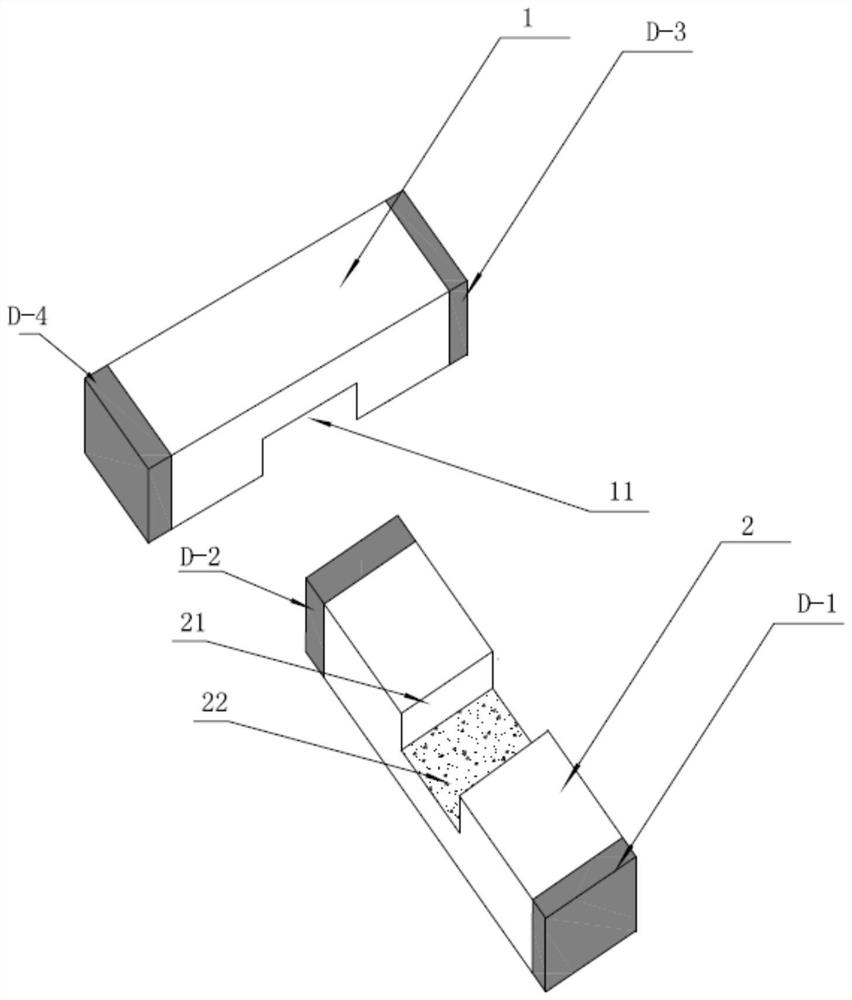
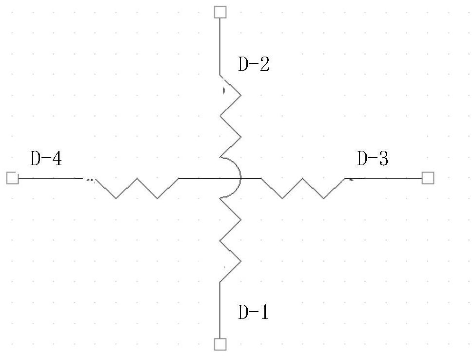
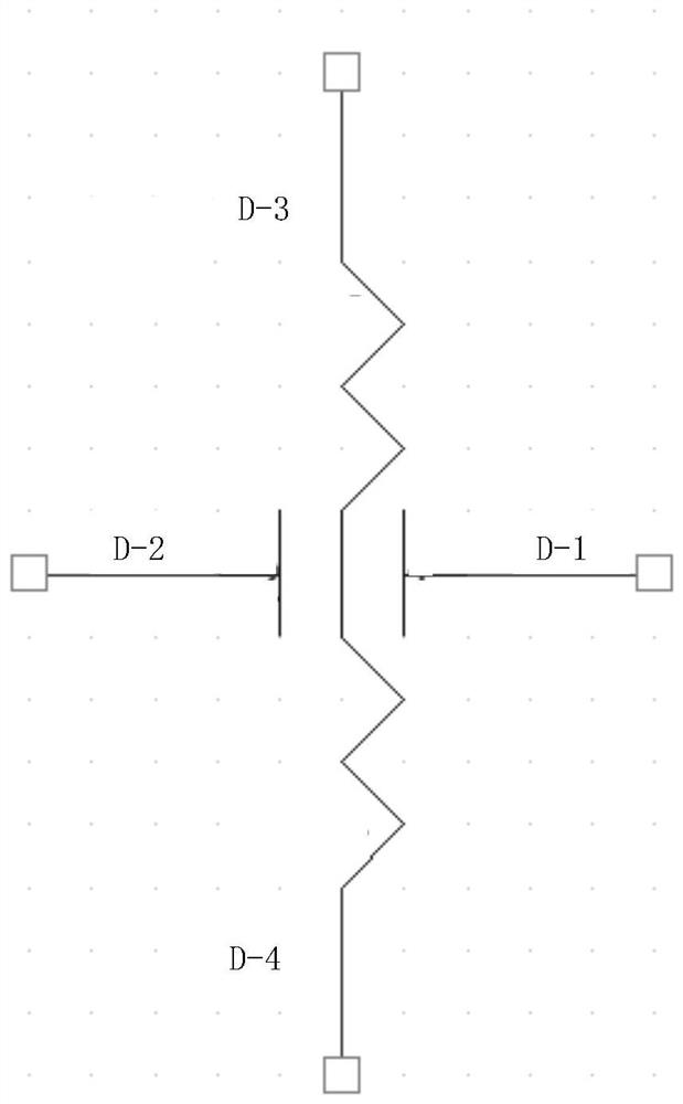
The embodiment of the invention discloses a chip component and its manufacturing method, and a method of manufacturing a four-electrode chip resistor. The chip component includes a component body and a zero-ohm chip resistor fixedly connected to the body. The zero-ohm The pad connection line of the chip resistor body is perpendicular to the pad connection line of the body, and an insulating material is provided between the component body and the zero-ohm chip resistor body. The present invention fixes and insulates a zero-ohm patch resistor body on the top (or bottom) of the original component body to form a bidirectional chip component with four electrodes, increasing the number of resistor layers and increasing the direction from the resistance design, which is quite Because it is possible to add a layer of wiring on the top or bottom layer of the PCB, it effectively solves the problem of difficult wiring, simplifies the wiring process, and improves wiring efficiency.

Description

technical field [0001] The invention relates to the technical field of surface mount device design, in particular to a patch component and a manufacturing method thereof, and a manufacturing method of a four-electrode chip resistor. Background technique [0002] At present, the reliability and cost of circuit board design is an extremely important part in server power supply design and other server circuit designs. PCB (Printed Circuit Board, printed circuit board) design is related to the success or failure of the entire design. At present, the requirements for the board area and the number of layers in PCB design are becoming increasingly stringent, because the larger the PCB area and the more layers, the higher the cost of the entire PCB. [0003] Therefore, a large part of the layout (layout) engineer's energy is considered in the layout and routing. At present, the way to cross the component routing in the circuit routing is mainly to make jumper routing through 0 ohm r...

Claims


Application Information

Patent Timeline
Patent Type & Authority Patents(China)
IPC IPC(8): H01C7/00H01C13/02H01C17/08H01C17/30
CPCH01C7/006H01C13/02H01C17/08H01C17/30
Inventor 陈安张洪镇肖波李松磊
Owner INSPUR SUZHOU INTELLIGENT TECH CO LTD
Why Eureka
Try Eureka