Graphic substrate, epitaxial wafer, manufacturing method, storage medium and LED chip

A patterned substrate and manufacturing method technology, applied in the direction of semiconductor devices, electrical components, circuits, etc., can solve the problems of uneven wavelength, uneven thickness of epitaxial layer, etc., to improve the uneven wavelength, improve the uneven thickness, improve Effect of Wavelength Uniformity

Active Publication Date: 2019-08-30
KONKA GROUP
View PDF11 Cites 2 Cited by
  • Summary
  • Abstract
  • Description
  • Claims
  • Application Information

AI Technical Summary

Problems solved by technology

[0008] Based on this, it is necessary to provide a patterned substrate, an epitaxial wafer, a manufacturing method, a storage medium, and an LED chip for the above-mentioned technical problems, aiming at solving the problem of the thickness of the epitaxial layer caused by the high-speed rotation of the LED epitaxial plate in the MOCVD furnace in the prior art. Non-uniform, which leads to the problem of non-uniform wavelength

Method used


Image

  • Graphic substrate, epitaxial wafer, manufacturing method, storage medium and LED chip
  • Graphic substrate, epitaxial wafer, manufacturing method, storage medium and LED chip
  • Graphic substrate, epitaxial wafer, manufacturing method, storage medium and LED chip

Examples


Embodiment Construction

[0026] In order to make the object, technical solution and advantages of the present invention clearer, the present invention will be further described in detail below in conjunction with the accompanying drawings and embodiments. It should be understood that the specific embodiments described here are only used to explain the present invention, not to limit the present invention.

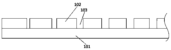
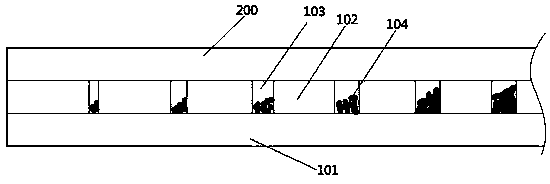
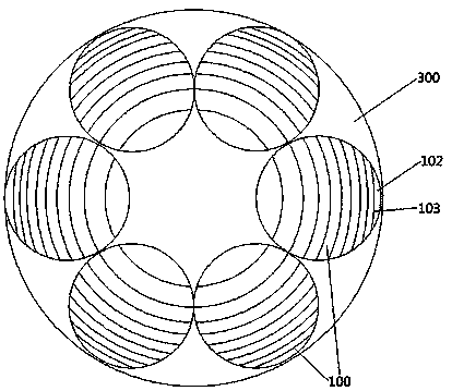
[0027] The patterned substrate 100 provided by the present invention (in image 3 Among them, 300 represents the carrier in MOCVD, and the six circles placed on the carrier 300 represent the patterned substrate 100. It can be understood that the number of patterned substrates 100 that can be accommodated in the carrier 300 can be increased. Minus, by no means limited to six), applied to Micro LED, such as figure 1 , figure 2 and image 3 As shown, it includes: a substrate body 101, at least one accommodating groove 103 is arranged above the substrate body 101, and the accommodating groove 103 h...


PUM


Abstract

The invention relates to a graphic substrate, an epitaxial wafer, a manufacturing method, a storage medium and an LED chip. The graphic substrate is applied to a Micro LED, and the body is provided with at least one accommodating groove for accommodating at least a portion of the epitaxial material dropped in the epitaxial process. The graphic substrate is advantaged in that at least a portion ofthe excess epitaxial material generated during high-speed rotational molding of the epitaxial layer in an MOCVD furnace can be dropped into the accommodating groove without remaining on the epitaxiallayer, a problem of uneven thickness of the epitaxial layer is ameliorated, wavelength uniformity is improved, and a problem of wavelength non-uniformity is at least solved.

Description

technical field [0001] The invention relates to the technical field of LEDs, in particular to a patterned substrate, an epitaxial wafer, a manufacturing method, a storage medium and an LED chip. Background technique [0002] Micro LED (miniature light-emitting diode) technology, that is, LED miniaturization matrix technology, refers to the integration of high-density micro-sized LED arrays on a chip; each pixel of the LED display can be addressed and individually driven to light up, Micro LED display It can be regarded as a miniature version of the outdoor LED display, reducing the pixel distance from millimeters to microns. [0003] Micro LED has many advantages. It has the advantages of high efficiency, high brightness, high reliability and fast response time of inorganic LED, and has the characteristics of self-illumination without backlight, and has the advantages of energy saving, small size and simple mechanism. [0004] Usually, the manufacturing method of Micro LED ...

Claims


Application Information

Patent Timeline
Patent Type & Authority Applications(China)
IPC IPC(8): H01L33/20H01L33/00
CPCH01L33/20H01L33/0075H01L33/007H01L33/32H01L33/12
Inventor 林伟瀚杨梅慧梁邦兵杨鑫
Owner KONKA GROUP
Why Eureka
Try Eureka