Broadband wave absorber and broadband wave absorber array based on resistive film

A technology of resistive film and wave absorber, applied in the field of electromagnetic field and microwave, can solve the problems of not too high wave absorption rate and limited bandwidth, and achieve the effect of high wave absorption rate, wide bandwidth and good angle stability

Active Publication Date: 2019-08-30
NANJING UNIV OF AERONAUTICS & ASTRONAUTICS
View PDF12 Cites 10 Cited by
  • Summary
  • Abstract
  • Description
  • Claims
  • Application Information

AI Technical Summary

Problems solved by technology

In the pursuit of wider and stronger absorbing performance, when traditionally using lumped elements to achieve absorbing effects, the bandwidth achieved is very limited, and the absorbing rate is often not too high

Method used


Image

  • Broadband wave absorber and broadband wave absorber array based on resistive film
  • Broadband wave absorber and broadband wave absorber array based on resistive film
  • Broadband wave absorber and broadband wave absorber array based on resistive film

Examples


Embodiment Construction

[0018] Embodiments of the invention are described in detail below, examples of which are illustrated in the accompanying drawings. The embodiments described below by referring to the figures are exemplary only for explaining the present invention and should not be construed as limiting the present invention.

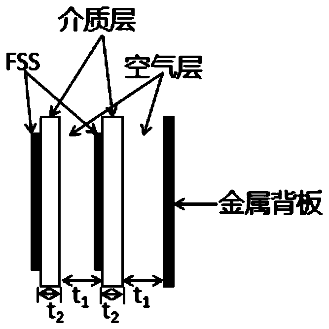
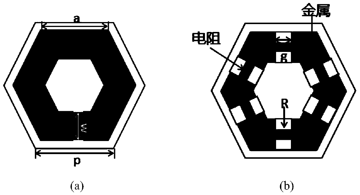
[0019] Such as figure 1 , figure 2 As shown in (a) and (b), the resistive film-based broadband absorber unit structure of the embodiment of the present invention includes a resistive film layer on the top layer, a resistive layer on the middle layer and a metal back plate on the bottom layer. The periodic structural unit of the resistive mold layer includes a hexagonal dielectric substrate and a hexagonal resistive film ring on the substrate; the metallic periodic structural unit of the resistive layer includes a hexagonal dielectric substrate and a hexagonal metal ring on the substrate. There is a resistor on the side of the strip. The total thickness of the absorbi...


PUM

PropertyMeasurementUnit
Thicknessaaaaaaaaaa
Lengthaaaaaaaaaa

Abstract

The invention discloses a broadband wave absorber and broadband wave absorber array based on a resistive film. The broadband wave absorber based on the resistive film is composed of a top resistive film layer, an intermediate resistive layer, a bottom metal backboard and two air layers between the three layers, wherein the resistive film layer is composed of a hexagonal dielectric substrate and ahexagonal resistive film ring, and the resistive layer is composed of a hexagonal dielectric substrate and a hexagonal metal ring loaded with resistance. The broadband wave absorber array adopts triangular periodic arrangement, which has better angular stability compared with common quadrilateral periodic arrangement. Compared with the common wave absorber loaded with lumped resistance, the broadband wave absorber has wider wave absorbing bandwidth and wave absorbing rate, thereby having important application prospects in stealth technology, electromagnetic compatibility and radar wave absorbing technology.

Description

technical field [0001] The invention relates to a broadband wave absorber and a broadband wave absorber array based on a resistive film, and belongs to the technical field of electromagnetic fields and microwaves. Background technique [0002] The so-called electromagnetic wave-absorbing structure refers to a class of materials that can absorb most of the electromagnetic wave energy irradiated on its surface and convert it into other forms of energy (mainly heat energy) with almost no reflection. The study of the absorbing structure starts with the Salisbury screen and the Jaumann absorber. A Salisbury screen or a Jaumann absorber can be formed by placing one or two resistive layers of appropriate resistance in front of a metal floor. They are all selective electromagnetic wave absorbers. Due to the unique frequency selection characteristics, structural form and specific frequency design characteristics of the Salisbury screen, it quickly attracted attention, and also prov...

Claims


Application Information

Patent Timeline
IPC IPC(8): H01Q17/00
CPCH01Q17/008
Inventor 王毅李靖曹群生
Owner NANJING UNIV OF AERONAUTICS & ASTRONAUTICS
Why Eureka
Try Eureka