Display module and display device

A technology for display modules and display areas, applied in instruments, digital data processing components, electrical solid-state devices, etc. Strong bending ability, avoid breakage, and ensure the effect of bending yield

Active Publication Date: 2019-09-10
BOE TECH GRP CO LTD +1
View PDF6 Cites 22 Cited by
  • Summary
  • Abstract
  • Description
  • Claims
  • Application Information

AI Technical Summary

Problems solved by technology

[0002] At present, OLED full-screen adopts the pad folding scheme to reduce the display frame. Pad folding involves the definition of the bending area. The film layer structure in the bending area has special treatment. The metal wiring in the bending area has better bending resistance, while Each film layer on the non-bending area shrinks 0.2mm from the boundary of the packaging area of ​​the display screen, and will not cover the bending area. When the PAD is bent, not only the part of the display panel in the bending area will be bent and deformed , the position adjacent to the non-bending area and the bending area, and even the entire display panel will be deformed. The bending yield of the module decreases, so how to improve the bending yield of the display module is a technical problem that those skilled in the art need to solve urgently

Method used


Image

  • Display module and display device
  • Display module and display device
  • Display module and display device

Examples


Embodiment Construction

[0025] In order to further explain the technical means and effects of the present invention to achieve the intended purpose of the invention, the specific implementation, structure, Features and their functions are described in detail below.

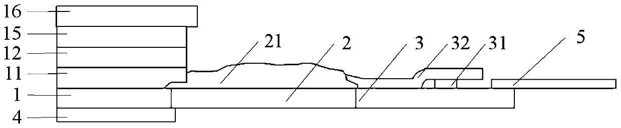
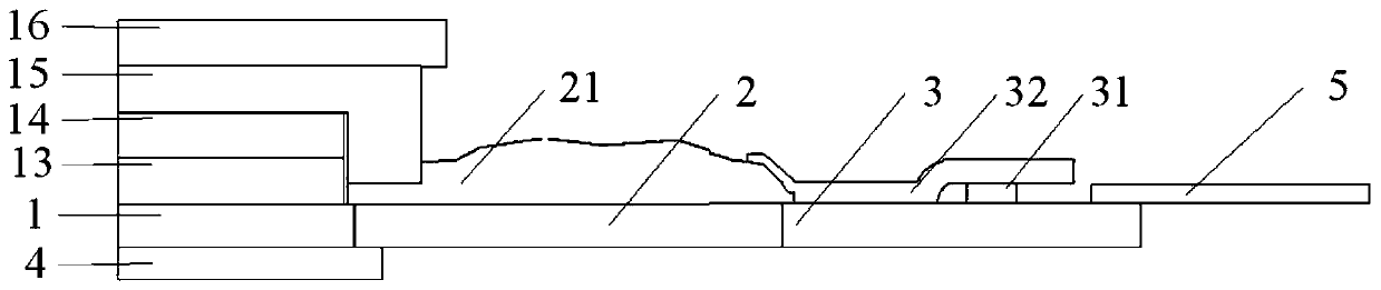
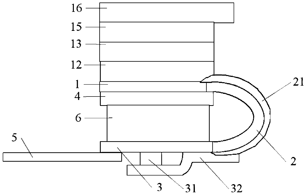
[0026] On the one hand, the embodiment of the present invention provides a display module, the display module includes: a display panel, such as Figure 1 to Figure 3 As shown, the display panel includes an effective display area 1, a bending area 2 and a liner area 3 arranged in sequence, an adhesive layer and a fixing layer are laminated on the effective display area 1 in sequence, and a protective adhesive layer is coated on the bending area 2 21. An electronic chip 31 is arranged on the pad area 3, and the electronic chip 31 is covered with a chip protection film 32. The chip protection film 32 extends to the protective adhesive layer 21 and covers the edge of the first side of the protective adhesive layer 21. The bonding layer ext...


PUM


Abstract

The invention discloses a display module and a display device, relates to the technical field of display and achieves the purpose of improving the bending yield of the display module. The main technical solution of the present invention comprises that the display module comprises a display panel, and the display panel comprises an effective display area, a bending area and a pad area arranged in sequence, wherein an adhesive layer and a fixed layer are sequentially laminated on the effective display area, and the bending area is coated with a protective adhesive layer. The pad area is providedwith an electronic chip, and the electronic chip is covered with a chip protective film, and the adhesive layer extends to the protective adhesive layer and covers the edge of a first side of the protective adhesive layer, and the edge of the adhesive layer is placed in the coverage area of the fixed layer, the chip protective film extends to the protective adhesive layer and covers the edge of asecond side of the protective adhesive layer, wherein the first side and the second side are opposite sides of the protective adhesive layer, the first side is adjacent to the effective display areaand the second side is adjacent to the pad area.

Description

technical field [0001] The invention relates to the field of display technology, in particular to a display module and a display device. Background technique [0002] At present, OLED full-screen adopts the pad folding scheme to reduce the display frame. Pad folding involves the definition of the bending area. The film layer structure in the bending area has special treatment. The metal wiring in the bending area has better bending resistance, while Each film layer on the non-bending area shrinks 0.2mm from the boundary of the packaging area of ​​the display screen, and will not cover the bending area. When the PAD is bent, not only the part of the display panel in the bending area will be bent and deformed , the position adjacent to the non-bending area and the bending area, and even the entire display panel will be deformed. The bending yield of the module decreases, so how to improve the bending yield of the display module is a technical problem urgently needed to be sol...

Claims


Application Information

Patent Timeline
Patent Type & Authority Applications(China)
IPC IPC(8): H01L51/52H01L27/32G06F1/16
CPCG06F1/1652H10K59/131H10K50/844H10K50/84
Inventor 杨恕权陈立强杨阳庞孟媛高洋
Owner BOE TECH GRP CO LTD
Why Eureka
Try Eureka