Circuit and method for supporting dual-path output of mainboard EDP and LVDS
A dual output and circuit technology, applied in TV, electrical components, color TV, etc., can solve the problems of poor user experience, low stability, high cost, etc., and achieve the effect of reducing cost and improving user experience
- Summary
- Abstract
- Description
- Claims
- Application Information
AI Technical Summary
Problems solved by technology
Method used
Image
Examples
Embodiment 1
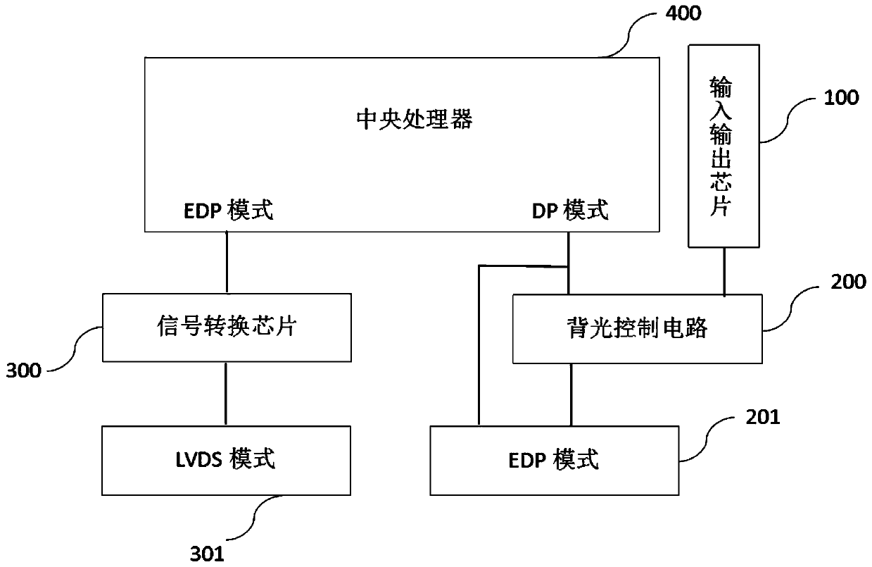
[0019] figure 1 Shown is the block diagram of the circuit supporting the main board EDP and LVDS dual output provided by Embodiment 1 of the present invention. For the convenience of description, only the parts related to the embodiment of the present invention are shown, and the details are as follows:
[0020] Including input and output chip 100 and backlight control circuit 200 and signal conversion chip 300; Signal conversion chip 300 is used to convert the video signal output of the EDP mode of CPU 400 output to the video signal output of LVDS mode 301; Backlight control circuit 200 is used for Adding a backlight control signal to the DP mode video signal output by the central processing unit 400; the input and output chip 100 is used to control the output voltage of the backlight control circuit 200;
[0021] Signal conversion chip 300 converts the video signal of the EDP mode that central processing unit 400 outputs to the video signal of LVDS mode 301, to realize the v...
Embodiment 2
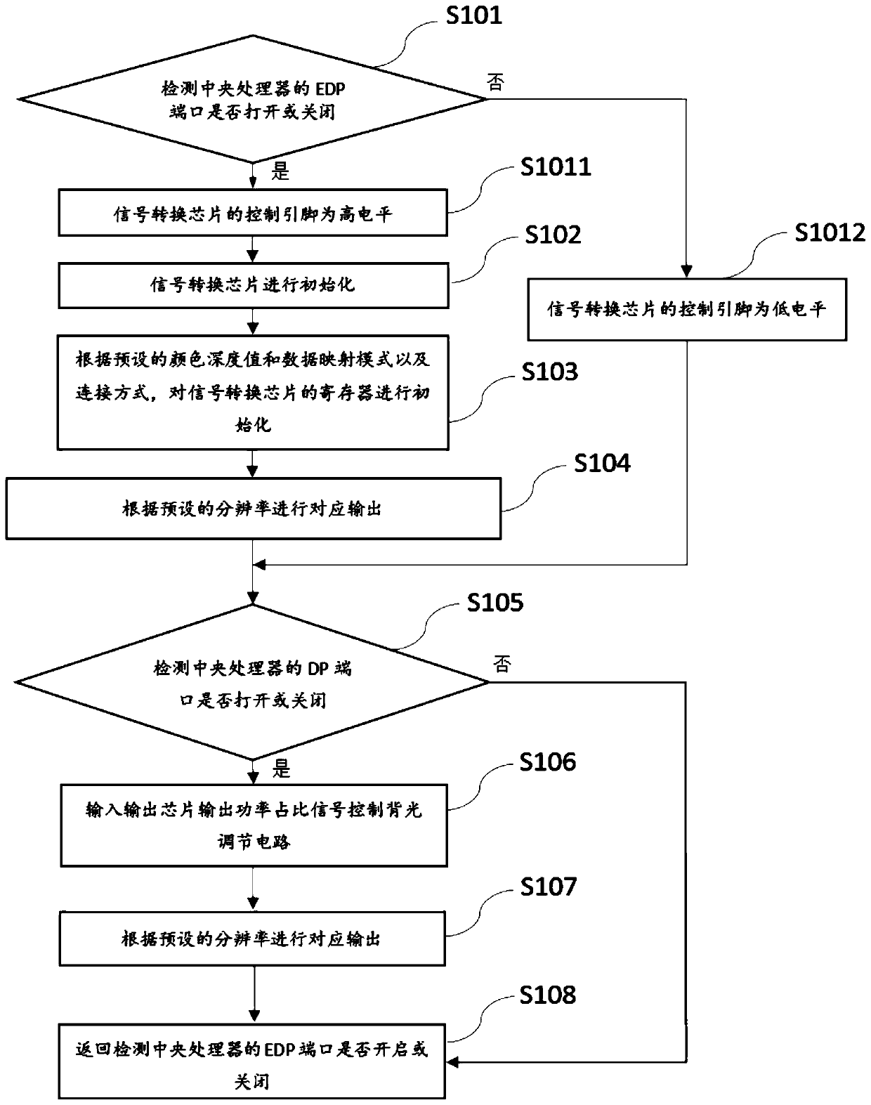
[0023] figure 2 It shows the implementation flow of the method for supporting the mainboard EDP and LVDS dual output provided by Embodiment 2 of the present invention. For the convenience of description, only the parts related to the embodiment of the present invention are shown, and the details are as follows:
[0024] In step S101, it is detected whether the EDP port of the central processing unit is opened or closed.
[0025] In step S1011, the control pin of the signal conversion chip is at a high level;
[0026] In the embodiment of the present invention, after detecting that the EDP port of the central processing unit is opened, the control pin of the signal conversion chip is at a high level.
[0027] In step S1012, the control pin of the signal conversion chip is low level;
[0028] In an embodiment of the present invention, after detecting that the EDP port of the central processing unit is closed, the control pin of the signal conversion chip is at a low level, an...
PUM
 Abstract
Description
Claims
Application Information

