Semiconductor production line MES and experiment method thereof

An experimental method and production line technology, applied in semiconductor/solid-state device manufacturing, electrical components, circuits, etc., can solve a large number of manual operations and other problems, and achieve the effect of improving overall production efficiency

Inactive Publication Date: 2019-09-13
华经智能信息(江苏)有限公司
View PDF5 Cites 8 Cited by
  • Summary
  • Abstract
  • Description
  • Claims
  • Application Information

AI Technical Summary

Problems solved by technology

[0016] Although it is a fully automatic production line, it still requires a lot of manual operation

Method used


Image

  • Semiconductor production line MES and experiment method thereof
  • Semiconductor production line MES and experiment method thereof
  • Semiconductor production line MES and experiment method thereof

Examples


Embodiment Construction

[0035] The present invention will be further described below in conjunction with accompanying drawing and embodiment:

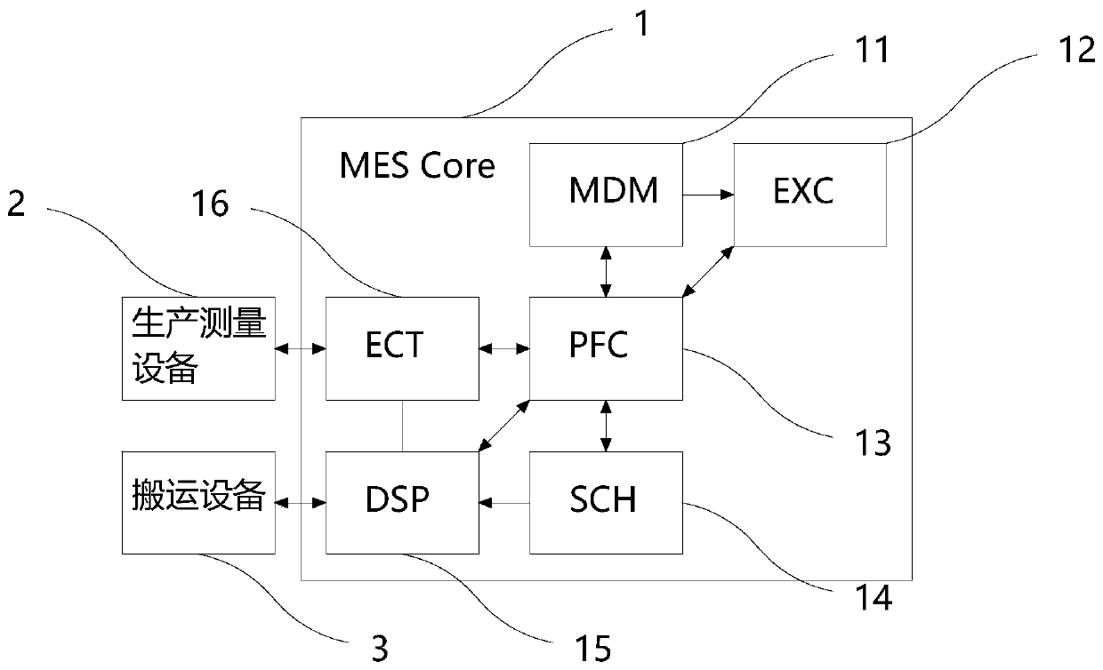
[0036] figure 1 It is a system block diagram of the semiconductor production line MES system of the present invention, please refer to figure 1 , a semiconductor production line MES system, including: MES core 1, MES core 1 includes: process flow control module 13 respectively communicates with equipment communication terminal 16, master data management module 11, scheduler 15, scheduler module 14, wherein, also An experiment management module 12 is included, and the experiment management module 12 communicates with the master data management module 11 and the technological process control module 13 .

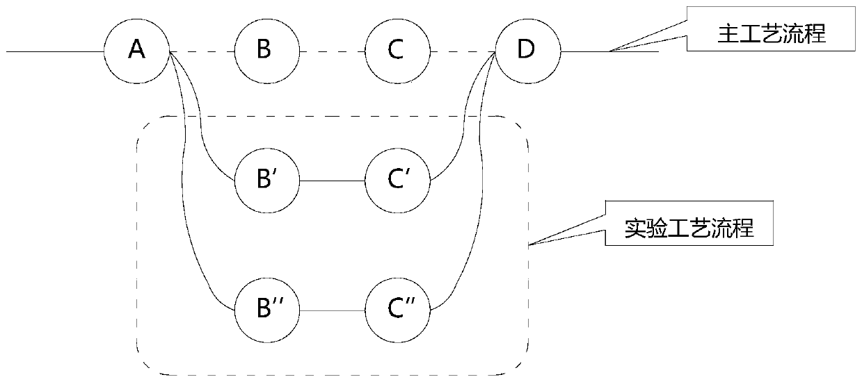
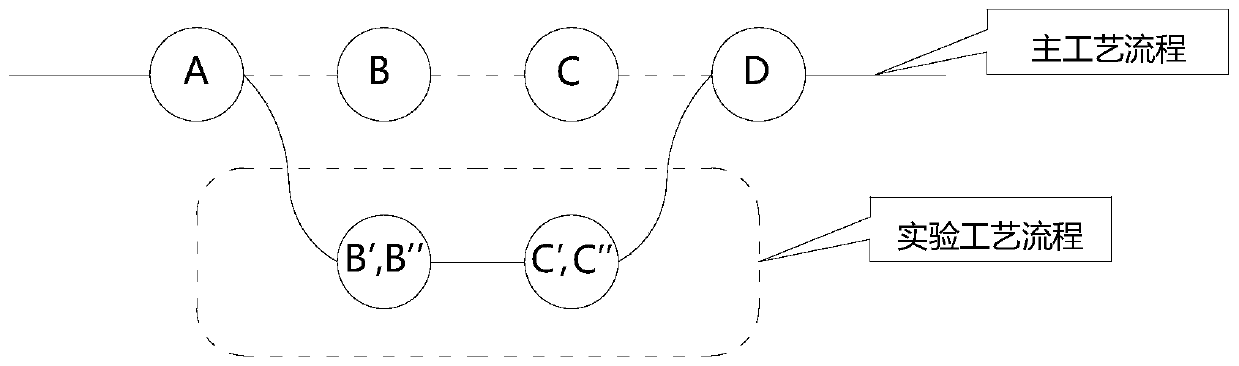
[0037] The present invention adds a functional module of experiment management to the MES system, which is relatively independent from other modules in the MES system, and is managed through the setting of the experiment process. The experimental process is ...


PUM


Abstract

The invention discloses a semiconductor production line MES. The MES comprises an MES core; the MES core comprises a technological process control module which communicates with an equipment communication terminal, a main data management module, a scheduler and a scheduling program module, and further comprises an experiment management module which communicates with the main data management moduleand the technological process control module. An experiment method of the semiconductor production line MES comprises the following steps: the experiment management module acquires a main technological process in the MES; and the experiment management module replaces one or more process steps in the main technological process with experiment process steps. The independent experiment management module is additionally arranged in an existing MES; and the experiment management module can obtain the main technological process, and can replace the process steps in the main technological process with the experiment process steps according to the need, so that an automatic experiment mode can be carried out on the basis of a non-stop condition.

Description

technical field [0001] The invention relates to a semiconductor system and an experimental method, in particular to a semiconductor production line MES system and an experimental method. Background technique [0002] The manufacturing process of semiconductors is complex, and the process can reach hundreds of steps. The transistors, diodes, capacitors, resistors, etc. on the wafer are formed by repeatedly covering the wafer with a thin film of special materials and then etching. Therefore, the thickness of the coating and the thickness after etching are crucial to product quality and precision, and are important recipe (menu: every step of the wafer processing specification in the production process) parameters. [0003] The MES system in the semiconductor industry (Manufacturing Execution System, that is, the production process execution system of the manufacturing enterprise, is a set of production information management system oriented to the execution layer of the worksh...

Claims


Application Information

Patent Timeline
Patent Type & Authority Applications(China)
IPC IPC(8): H01L21/67
CPCH01L21/67253H01L21/67276
Inventor 冯宇夏利敏崔琴
Owner 华经智能信息(江苏)有限公司
Why Eureka
Try Eureka