Wafer box

A wafer box and wafer technology, applied in the direction of electrical components, semiconductor/solid-state device manufacturing, circuits, etc., can solve problems such as damage, jitter, and shaking out of the wafer box, so as to avoid position shifting and reduce The effect of small jitter amplitude and reasonable structure design

Pending Publication Date: 2019-09-17
JIANGSU SEVEN DIMENSIONAL TEST TECH CO LTD
View PDF0 Cites 1 Cited by
  • Summary
  • Abstract
  • Description
  • Claims
  • Application Information

AI Technical Summary

Problems solved by technology

At present, the structure design of the existing wafer box is unreasonable. In the semiconductor processing process, the wafer box containing the wafers to be processed is usually temporarily stored in the buffer storage area of ​​the processing equipment, and the wafer box is transported by the conveying mechanism parallel to it. The wafers in the round box are grabbed and transported to the next process in sequence. During this process, the processing equipment shakes due to the dynamic and static assembly of the driving device in the working state, and the wafer box in the buffer storage area is also shaken. , causing the wafers in the wafer box to be displaced and dislocated due to long-term shaking, and some may even shake out of the wafer box and collide with the conveying mechanism next to the wafer box (such as figure 1 As shown, among them: wafer box 1; wafer 2; conveying mechanism 3), damage occurred

Method used


Image

  • Wafer box
  • Wafer box
  • Wafer box

Examples


Embodiment Construction

[0044] The following will clearly and completely describe the technical solutions in the embodiments of the present invention with reference to the accompanying drawings in the embodiments of the present invention. Obviously, the described embodiments are only part of the embodiments of the invention, not all of them. Based on the embodiments of the present invention, all other embodiments obtained by persons of ordinary skill in the art without making creative efforts belong to the protection scope of the present invention.

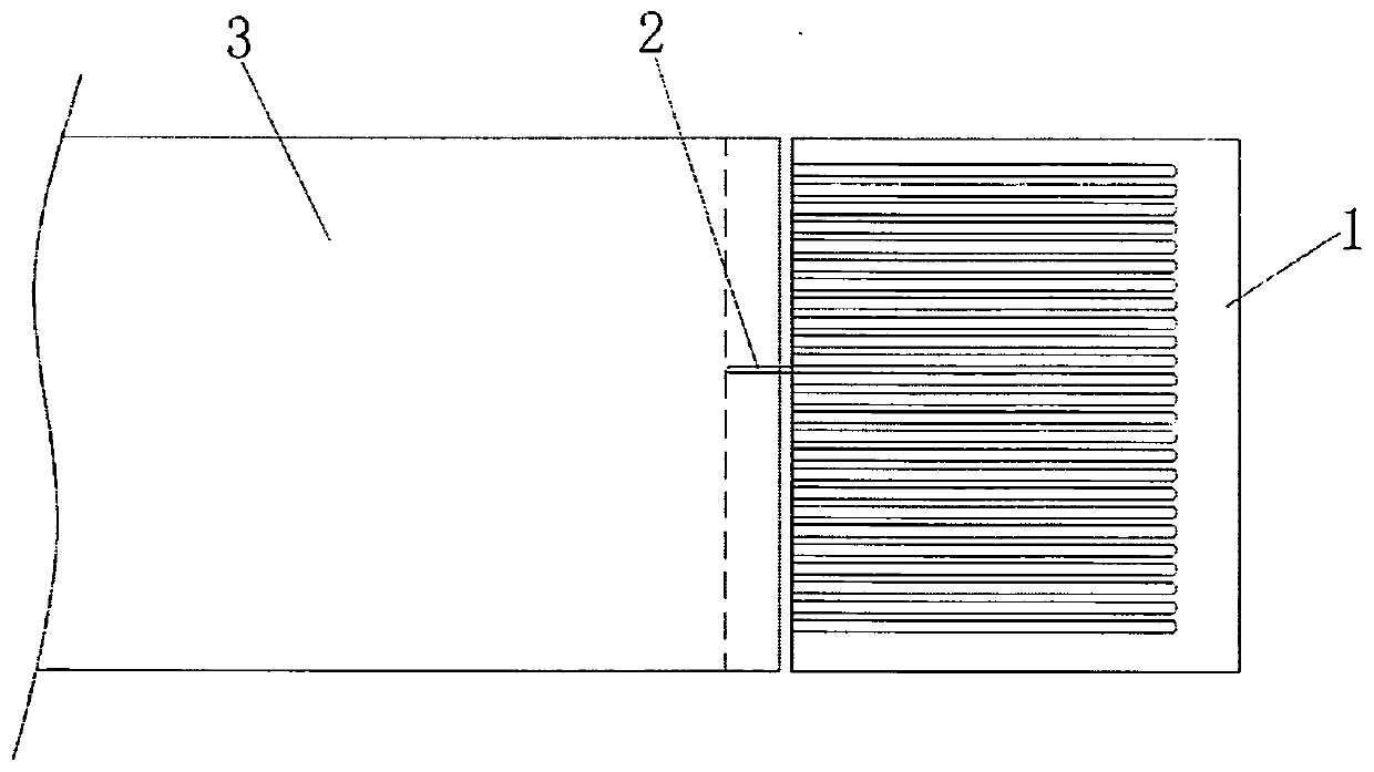
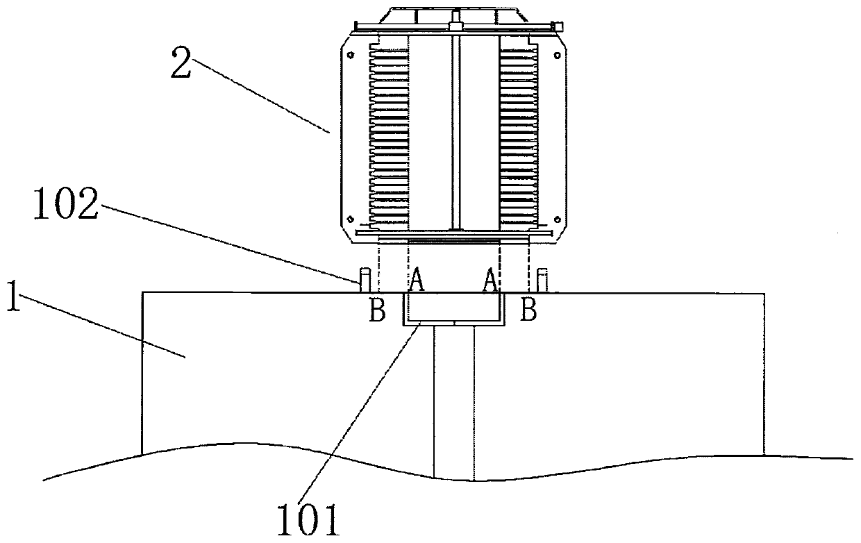
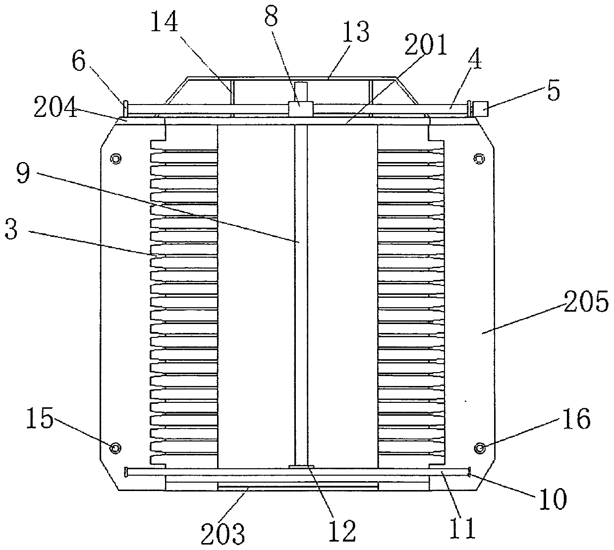
[0045] see Figure 1-Figure 6 , a kind of wafer box that the present invention relates to includes a wafer box body 2 placed on the machine platform 1, the wafer box body 2 includes a chassis 204, and a support frame is arranged on the chassis 204, and the support frame It includes a top plate 201 and two symmetrical upright side plates 202. The left and right sides of the top plate 201 are respectively connected to the tops of the two side plates 202. T...


PUM


Abstract

The invention relates to a wafer box. The wafer box comprises a wafer box body placed on a machine table. The wafer box body comprises a chassis. A supporting framework is arranged on the chassis. The supporting framework comprises a top plate and two left-right symmetrical vertical side plates. A plurality of bearing strips are arranged on the inner side faces of the side plates from top to bottom at intervals. The bearing strips on the left and right sides are in one-to-one correspondence. A transverse lead screw is arranged above of the top plate. A driving motor is arranged at one end of the screw rod. The screw rod is sleeved in a nut base. The front side of the nut base extends forwards and is provided with a connecting part. A stop rod extending downwards is arranged in the connecting part in a penetrating mode. A transverse linear guide rail is arranged below the stop rod. A sliding base is arranged on the linear guide rail. The top face of the sliding base is connected with the bottom end of the stop rod. The wafer box is reasonable in structural design, the wafers can be prevented from being shaken off and damaged, and the rejection rate is reduced.

Description

technical field [0001] The invention relates to a wafer box, which belongs to the technical field of semiconductor manufacturing. Background technique [0002] Wafer refers to the silicon wafer used in the production of silicon semiconductor integrated circuits. Because of its circular shape, it is called a wafer. It can be processed into various circuit element structures on the silicon wafer and become an IC with specific electrical functions. product. In order to ensure the safe storage, transportation, and handling of wafers, wafer boxes are widely used as wafer carrying and transportation tools, so that wafers can be well protected. At present, the structure design of the existing wafer box is unreasonable. In the semiconductor processing process, the wafer box containing the wafers to be processed is usually temporarily stored in the buffer storage area of ​​the processing equipment, and the wafer box is transported by the conveying mechanism parallel to it. The wafe...

Claims


Application Information

Patent Timeline
Patent Type & Authority Applications(China)
IPC IPC(8): H01L21/673
CPCH01L21/67333
Inventor 邹桂明常兵杭晓宇吴晓杰施明明
Owner JIANGSU SEVEN DIMENSIONAL TEST TECH CO LTD
Why Eureka
Try Eureka