Organic light-emitting diode (OLED) device including mixed covering layer

A technology of electroluminescent devices and covering layers, which is applied in the direction of electric solid devices, electrical components, semiconductor devices, etc., can solve the problems of reducing the light extraction efficiency of organic electroluminescent devices, so as to improve the light extraction efficiency and reduce the overall surface area of ​​the interface. Chance of reflection, effects that increase extraction strength

Inactive Publication Date: 2019-09-24
JIANGSU SUNERA TECH CO LTD
View PDF9 Cites 6 Cited by
  • Summary
  • Abstract
  • Description
  • Claims
  • Application Information

AI Technical Summary

Problems solved by technology

It can be seen that total internal reflection occurring at these interfaces greatly reduces the light extr

Method used


Image

  • Organic light-emitting diode (OLED) device including mixed covering layer
  • Organic light-emitting diode (OLED) device including mixed covering layer
  • Organic light-emitting diode (OLED) device including mixed covering layer

Examples


Embodiment 1

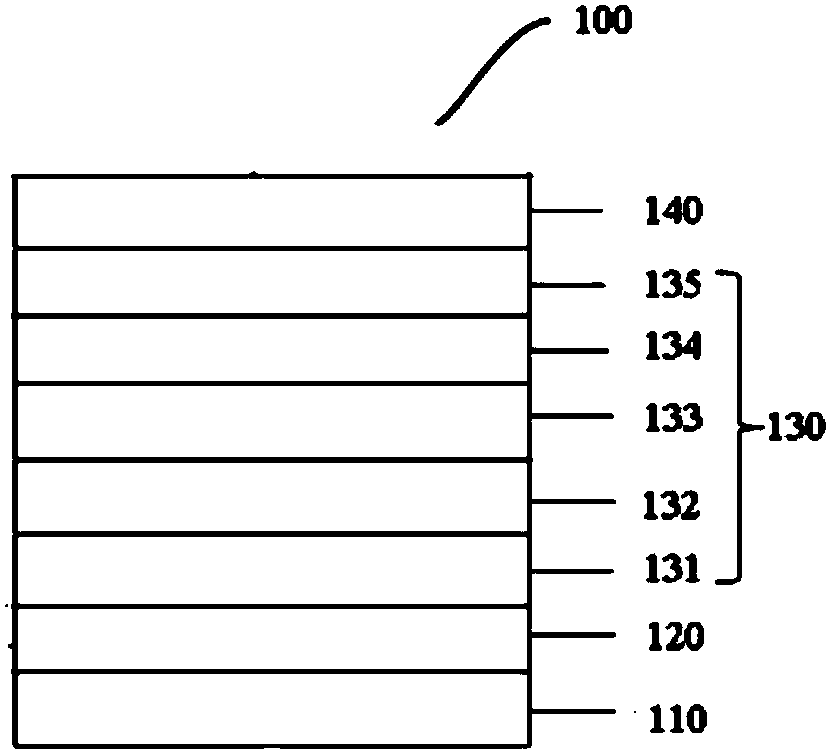
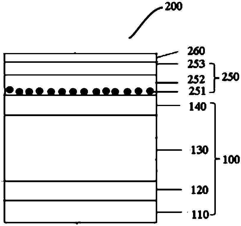
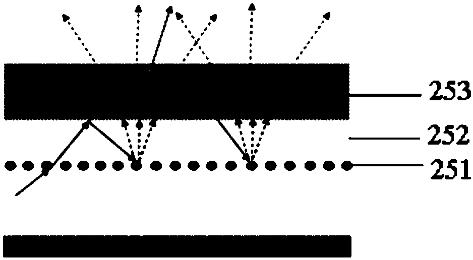
[0084] Embodiment 1: manufacture OLED device of the present invention

[0085] On the glass substrate (base layer 110), form the ITO opaque layer (reflective electrode layer 120) of 200nm by sputtering mode, and etch into the figure of demand, clean each 15 minutes respectively with deionized water, acetone, ethanol ultrasonically, then Treat in a plasma cleaner for 2 minutes; here the ITO electrode layer is the anode, and on the ITO anode layer, the hole injection layer material HAT-CN is evaporated by vacuum evaporation with a thickness of 10nm. This layer is used as a hole injection layer. Layer 131; on the hole injection layer 131, the hole transport layer material NPB is evaporated by vacuum evaporation, the thickness is 60nm, and this layer is the hole transport layer 132; on the hole transport layer 132, the green light emitting layer is evaporated Layer 133, CBP as host material, Ir(ppy) 3 As doping material, Ir(ppy) 3 The weight ratio to CBP is 1:9 (90wt% CBP), and ...


PUM

PropertyMeasurementUnit
The average particle sizeaaaaaaaaaa
Thicknessaaaaaaaaaa

Abstract

The invention provides an organic light-emitting diode (OLED) device including a mixed covering layer, wherein the mixed covering layer includes a particle scattering layer and a multilayer covering layer (such as a first covering sub-layer and a second covering sub-layer); the particle scattering layer is arranged between the first covering sub-layer and a top transparent electrode and in incompletely covered micro-nano particle distribution on the top transparent electrode; the first covering sub-layer is contacted with the top electrode and the particle scattering layer; and the refractive index of the first covering sub-layer is higher than that of the second covering sub-layer. The mixed covering layer in the device has an effect of improving the light extraction efficiency.

Description

technical field [0001] The present invention relates to an organic electroluminescent device (OLED device) with a hybrid covering layer and a method for its preparation. Background technique [0002] OLEDs generally include a substrate, a first electrode layer, an organic layer, and a second electrode layer. OLEDs can be classified into bottom emitting devices, top emitting devices, and side emitting devices. In a structure called a bottom emitting device, the first electrode layer may be formed as a transparent electrode layer, and the second electrode layer may be formed as a reflective electrode layer; in a structure called a top emitting device, the first electrode layer may be formed as a reflective electrode layer, and the second electrode layer may be formed as a transparent electrode layer; and in a structure called a two-sided light emitting device, both the first electrode layer and the second electrode layer may be transparent electrode layers. [0003] The ligh...

Claims


Application Information

Patent Timeline
IPC IPC(8): H01L51/52H01L51/56
CPCH10K50/854H10K71/00
Inventor 李宝雨李崇张兆超赵鑫栋
Owner JIANGSU SUNERA TECH CO LTD
Why Eureka
Try Eureka