Application of natural blue pigment in organic semiconductor device
A technology of organic semiconductor and blue pigment, which is applied in semiconductor devices, semiconductor/solid-state device manufacturing, electric solid-state devices, etc., can solve problems such as low processing temperature, and achieve the effect of high molar extinction coefficient
- Summary
- Abstract
- Description
- Claims
- Application Information
AI Technical Summary
Problems solved by technology
Method used
Image

Examples
preparation example Construction
[0040] Wherein, the preparation method of the semiconductor layer includes the steps of dissolving the natural blue pigment in the solution, and coating the solution on the substrate by spin coating or blade coating to form the semiconductor layer. The thickness of the semiconductor layer is 10 to 300 nm. Preferably, the thickness of the semiconductor layer is 20-80 nm.
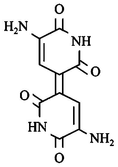
[0041]In the present invention, the preparation of natural blue pigment refers to the patent application number CN201210416265.0 "Synthetic method and extraction process of blue natural dye". Grow in LB broth (10 g / L tryptone, 5 g / L yeast extract and 10 g / L sodium chloride) at 37°C with shaking at 250 rpm. After the OD600 of the culture reached 0.4˜0.6, 200 μM IPTG was added to induce the expression of Sc-IndC (indigo structure synthetase) and subsequent production of natural blue pigment. The induced broth was maintained for another 36 hours at 18°C and 250 rpm. The natural blue pigment is then harveste...
Embodiment 1
[0042] Embodiment one elemental analysis:
[0043] The product obtained adopts element analyzer (EURO EA3000) to carry out carbon, hydrogen, nitrogen and sulfur elemental analysis, and the results are as follows:
[0044] element(%) nitrogen carbon hydrogen Average specific gravity 20,520 45,610 4,319 theoretical mean 22,565 48,394 3,249 Specific gravity difference -2,042 -2,784 1,07
[0045] In the present invention, the film used for optical measurement, cyclic voltammetry (CV) measurement and organic field effect transistor (OFET) characterization is to adopt organic evaporation system (Vaksis R&D and Engineering) to manufacture by physical vapor deposition, so as to realize the thickness precise control. Sublimation treatment is at 230-250°C, 10 -6 Under ultra-high vacuum conditions in the ceramic crucible (Al 2 o 3 ) is carried out below. Prior to deposition, the crucible was preheated to 230 °C with a closed substrate baff...
Embodiment 2
[0046] Embodiment 2 Spectral detection
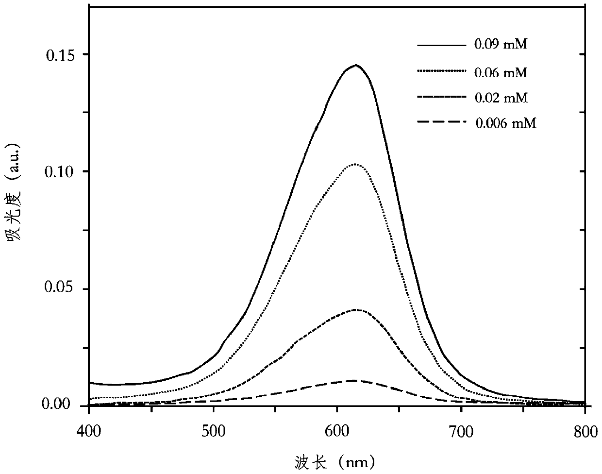
[0047] The material was analyzed by ultraviolet-visible light spectrum and fluorescence spectrum, 0.006mM, 0.02mM, 0.6mM and 0.9mM dimethyl sulfoxide solutions of natural blue pigment were prepared respectively, and the molar extinction coefficient was determined by Beer-Lambert method.
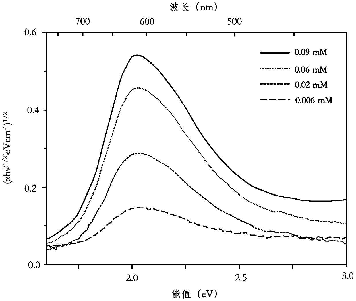
[0048] The new material measures the absorbance of ultraviolet and visible light in a certain frequency range, so as to obtain the basic data of its optical properties, such as Figure 2A . As long as the organic compound is excited by ultraviolet or visible light, the electronic energy change can be determined by absorbance measurement. The optical gap is determined by Tauc plot, as Figure 2B , through the energy distribution of monochromatic light, a linear absorption feature can be observed. Natural cyanine is a natural compound, so under its optical gap reference, the optical absorption should be cut off at around 1.7eV.
[0049] In order to e...
PUM
 Abstract
Description
Claims
Application Information
 - R&D Engineer
- R&D Manager
- IP Professional
- Industry Leading Data Capabilities
- Powerful AI technology
- Patent DNA Extraction
Browse by: Latest US Patents, China's latest patents, Technical Efficacy Thesaurus, Application Domain, Technology Topic.
© 2024 PatSnap. All rights reserved.Legal|Privacy policy|Modern Slavery Act Transparency Statement|Sitemap