Display panel and manufacturing method thereof
A technology for display panels and manufacturing methods, applied in semiconductor/solid-state device manufacturing, instruments, optics, etc., can solve problems such as cracking or breaking of metal electrodes, and achieve the effect of avoiding cracks or breaks and not being easy to break
- Summary
- Abstract
- Description
- Claims
- Application Information
AI Technical Summary
Problems solved by technology
Method used
Image
Examples
Embodiment Construction
[0038] The directional terms mentioned in the present invention, such as "up", "down", "front", "back", "left", "right", "inside", "outside", "side", etc., are only appended The directions in the drawings and the direction terms used herein are used to explain and illustrate the present invention, rather than to limit the protection scope of the present invention.
[0039] In addition, it should also be noted that in some alternative implementations, the steps of all methods described herein may occur out of order. For example, two steps shown in succession may, in fact, be executed substantially concurrently, or the two steps may sometimes be executed in the reverse order.
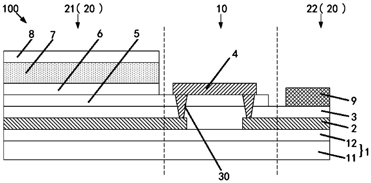
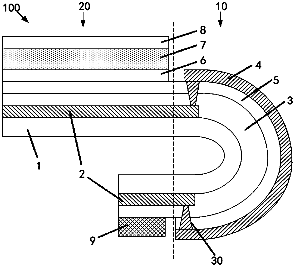
[0040] see figure 1 , figure 2 As shown, one embodiment of the present invention provides a display panel 100, which defines a bending area 10 and non-bending areas 20 located on both sides of the bending area 10, and the non-bending area 20 includes The displayed display area 21 and the binding area ...
PUM
 Abstract
Description
Claims
Application Information


