OLED (Organic Light-Emitting Diode) display panel

A display panel and array substrate technology, applied in the field of OLED display panels, can solve the problems of shortened screen life, vulnerability to environmental water and oxygen erosion, etc., and achieve the effect of prolonging the service life

Inactive Publication Date: 2019-10-22
WUHAN CHINA STAR OPTOELECTRONICS SEMICON DISPLAY TECH CO LTD
View PDF3 Cites 15 Cited by
  • Summary
  • Abstract
  • Description
  • Claims
  • Application Information

AI Technical Summary

Problems solved by technology

Therefore, when the subsequent process cuts the effective light-emitting area of ​​the OLED display panel along the edge of the opening area 9 to form a circular hole for placing the camera, a section will be formed on the multi-layer film layer, and the multi-layer film layer involved includes In the OLED functional layer 6, the organic common film layer and the metal common film

Method used


Image

  • OLED (Organic Light-Emitting Diode) display panel
  • OLED (Organic Light-Emitting Diode) display panel
  • OLED (Organic Light-Emitting Diode) display panel

Examples


Embodiment Construction

[0031] In order to further illustrate the technical means adopted by the present invention and its effects, the following describes in detail in conjunction with preferred embodiments of the present invention and accompanying drawings.

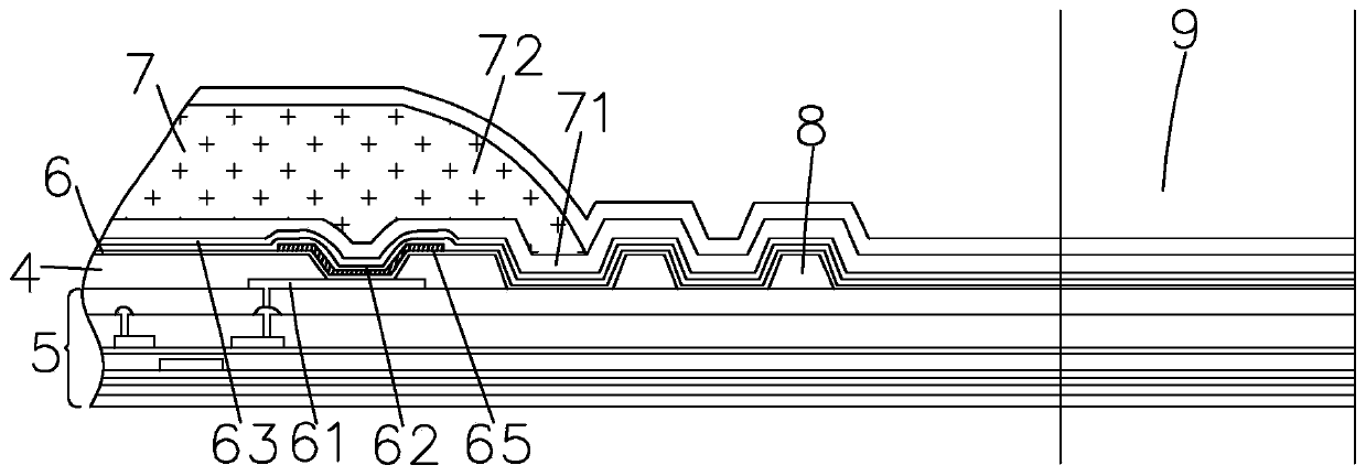
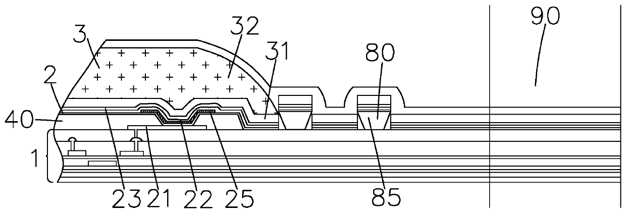
[0032] see image 3 , the first embodiment of the OLED display panel of the present invention, comprising an array substrate 1, an OLED functional layer 2 disposed on the array substrate 1, and a thin film encapsulation layer 3 covering the OLED functional layer 2 on the array substrate 1 .

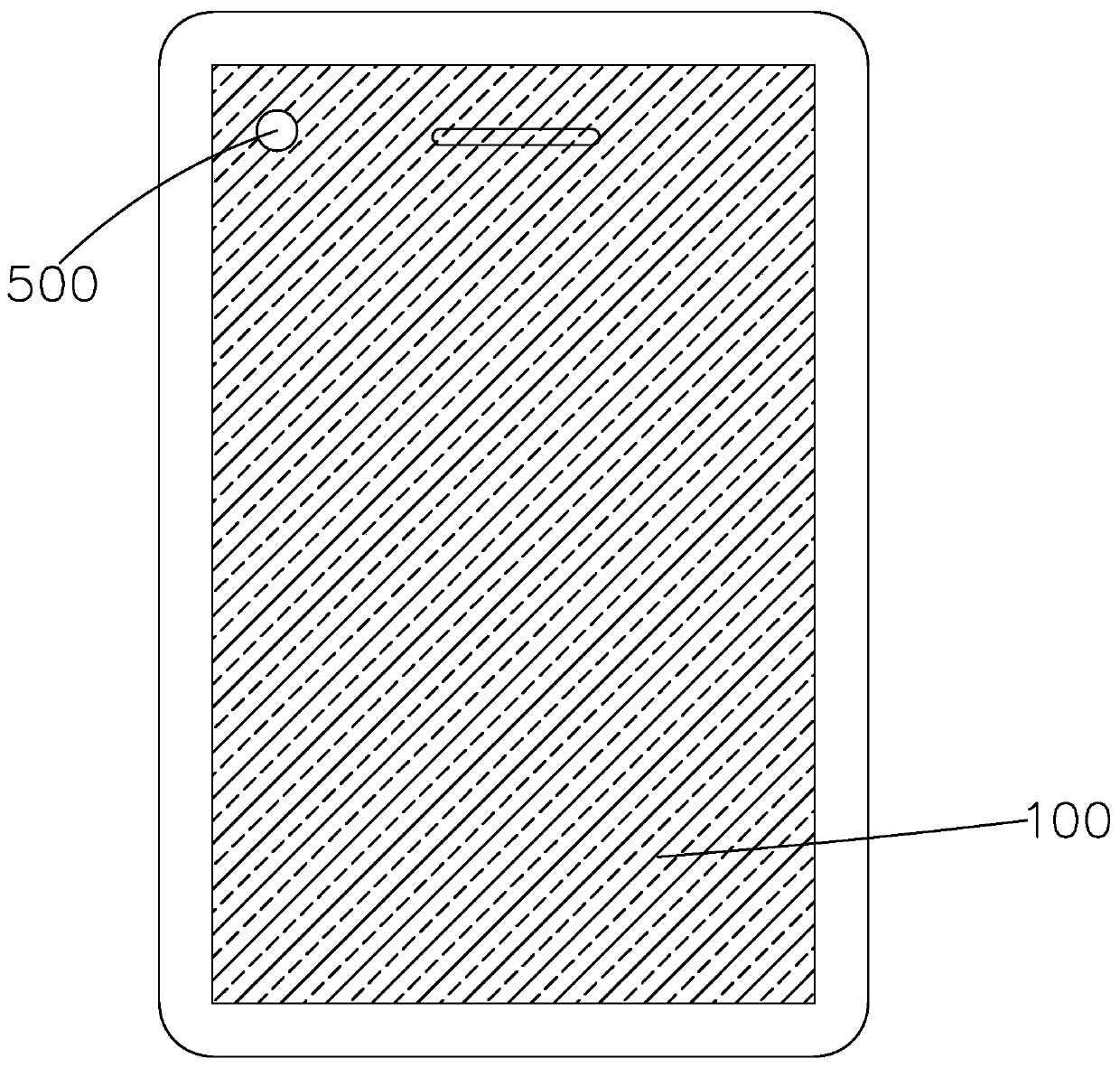
[0033] Specifically, the OLED display panel is provided with an opening area 90 to be cut and removed, and the opening area 90 is used to form an opening through the upper and lower surfaces of the OLED display panel for placing the camera after cutting.

[0034] Specifically, between the array substrate 1 and the OLED functional layer 2, a blocking dam 80 surrounding the opening area 90 is provided on the periphery of the opening area 90, and the blocki...


PUM


Abstract

The invention provides an OLED (Organic Light-Emitting Diode) display panel, which comprises an array substrate, an OLED functional layer and a thin-film packaging layer, and is characterized in thatthe OLED display panel is internally provided with an opening area to be cut and removed, a blocking dam surrounding the opening area is arranged between the array substrate and the OLED functional layer at the periphery of the opening area, the blocking dam includes a blocking unit with the cross section being in the shape of an inverted trapezoid around the opening area, and the OLED functionallayer above the blocking dam is disconnected at two sides of the blocking dam during film forming as the cross section of the blocking unit is in the shape of an inverted trapezoid. According to the invention, the structure of the blocking dam at the periphery of the opening area is optimized, and the cross section of the blocking unit is enabled to be in the shape of an inverted trapezoid, so that the whole common film layer deposited by a common mask plate can be cut off at two sides of the blocking dam, thus environmental water and oxygen can be prevented from invading into a light-emittingpixel area of the panel from the cutting section of the opening area along the continuous common film layer after the opening area is cut, and the service life of the panel is prolonged.

Description

technical field [0001] The invention relates to the field of display technology, in particular to an OLED display panel. Background technique [0002] In flat panel display technology, organic light-emitting diode (Organic Light-Emitting Diode, OLED) display has the advantages of thinness, active light emission, fast response speed, large viewing angle, wide color gamut, high brightness, low power consumption and the ability to prepare flexible screens. And many other excellent properties have aroused great interest in the scientific research community and the industry. [0003] Nowadays, the design of "full screen" has become the mainstream of the times. At present, all suppliers are focusing on the research and development of full-screen products with a higher screen-to-body ratio. For example, the special-shaped (Notch) screen design adopted by the iPhone X mobile phone. The recently emerging under-screen camera design is O-cut (O-Cut) screen design, such as figure 1 A...

Claims


Application Information

Patent Timeline
IPC IPC(8): H01L27/32
CPCH10K59/88H10K59/00H10K59/122H10K59/12
Inventor 蒋谦
Owner WUHAN CHINA STAR OPTOELECTRONICS SEMICON DISPLAY TECH CO LTD
Why Eureka
Try Eureka